
Quick Answer
Open ZenTimings on Ryzen system. Dashboard displays active primary, secondary, tertiary memory timings, bus clocks, voltages. Compare reported values directly against BIOS settings and kit specifications. Matching values confirm applied XMP or EXPO profiles. Discrepancies reveal motherboards reverting to default JEDEC speeds or unstable automatic subtiming training.
Pros
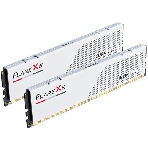
- 64GB kit with two 32GB DDR5 U-DIMM modules
- Rated up to 6000 MT/s with CL36-36-36-96 timings, per listing
- Includes AMD EXPO and Intel XMP 3.0 overclock profiles
- Matte white finish listed in specifications
- Non-ECC modules listed for desktop PCs
Cons
- Speeds above JEDEC default require BIOS overclocking
- Kits must be used as matched sets; mixing can cause instability

Pros
- High 64GB capacity across two 32GB UDIMM modules
- Operates at up to 5600MHz with downclocking support
- Low standard operating voltage of 1.1V
- Dual-rank (2Rx8) non-ECC desktop configuration
Cons
- Requires compatible DDR5-supported motherboard and CPU
- Lacks built-in RGB lighting for aesthetic customization

Pros
- E-ATX board for Intel Core Ultra Series 2 on LGA 1851
- Listed M.2 layout includes onboard and expander slots
- DDR5 listed up to 9200+ MT/s OC on four DIMM slots
- 3.99-inch LCD for hardware monitoring, per listing
- Thunderbolt 5 accessory card listed for rear ports
Cons
- Thunderbolt 5 relies on an accessory card, per listing
- E-ATX size and 6.8-pound weight may limit case options
What ZenTimings Shows
ZenTimings interrogates AMD System Management Unit (SMU) registers via kernel drivers. Utility extracts operational register states directly from memory controller. Engineering evaluations indicate zero synthetic calculation; software reflects real hardware configuration committed by AGESA firmware during memory training.
Dashboard delivers complete hardware telemetry across six main domains:
- Bus Clock Domain: Fabric Clock (FCLK), Memory Controller Clock (UCLK), Memory Clock (MCLK). Quantifies fabric-to-controller synchronization state.
- Primary Latencies: Core access cycles governing basic row/column read, write, precharge states (tCL, tRCDRD, tRCDWR, tRP, tRAS).
- Secondary and Tertiary Timings: Bank turnaround, row cycle periods, refresh cycles, bus turnaround delays (tRC, tRFC, tFAW, tRRD, tWTR, tRTP, tRDWR).
- Command Bus Settings: Command Rate (CR), Gear Down Mode (GDM), Power Down Enable (PDE).
- Impedance and Drive Strengths: On-Die Termination (RTT_NOM, RTT_WR, RTT_PARK) plus processor output impedance (ProcODT) and CAD bus drive strengths (ClkDrvStr, AddrCmdDrvStr, CsOdtDrvStr, CkeDrvStr) calibrated in ohms (Ω).
- Voltage Rail Readouts: SoC Voltage (VSOC), Memory Controller I/O (VDDG CCD, VDDG IOD), PHY interface (CLDO VDDP), Module supply rail (VDD/VDDQ/VPP).
Reading Primary Timings
Primary timings dictate absolute cycle count between memory controller state requests and DRAM internal bank execution. Timings scale inversely with clock frequency; raw latency calculation equals: Cycle Time (ns) = (Timing Clocks × 2000) / Data Rate (MT/s).
| Timing Parameter | Register Name | Functional Definition | Typical Safe Baseline |
|---|---|---|---|
| CAS Latency | tCL | Clocks between column read command and first word of data burst out. | 14-18 (DDR4-3600) / 30-36 (DDR5-6000) |
| RAS to CAS Read Delay | tRCDRD | Clocks to open active row and access column for read operations. Dictated by silicon binning. | 14-19 (DDR4) / 36-40 (DDR5) |
| RAS to CAS Write Delay | tRCDWR | Clocks between row active command and column write strobe. Tolerates tight clock counts. | 8-16 (DDR4) / 30-38 (DDR5) |
| Row Precharge Delay | tRP | Clocks required to precharge open bank line, clearing charge for next access. | 14-19 (DDR4) / 36-40 (DDR5) |
| Row Active Time | tRAS | Minimum clocks bank line must remain open before precharge cycle starts. | 28-36 (DDR4) / 28-42 (DDR5) |
| Gear Down Mode / Command Rate | GDM / CR | GDM latches command/address bus every second clock. CR sets chip select duration (1T vs 2T). | GDM Enabled (1T bus latching) |
Read primary values directly. Mismatched tRCDRD and tRCDWR values indicate asynchronous read/write routing. Samsung 8Gb B-die allows flat primaries (e.g., 14-14-14-14-28). SK Hynix (DJR, M-die, A-die) and Micron dies require elevated tRCDRD relative to tCL. GDM enabled forces tCL to even integers; setting tCL 15 with GDM enabled forces hardware to train at tCL 16.
Secondary and Tertiary Timings
Secondary timings control overall bus throughput, page contention, and internal capacitor refresh intervals. Poor secondary parameters degrade operational efficiency regardless of low CAS latency.
- tRC (Row Cycle Time): Clocks for complete open-refresh-close cycle in single bank. Mathematical floor:
tRC = tRAS + tRP. Setting tRC below theoretical floor causes immediate memory parity exceptions. - tRFC / tRFC2 / tRFCsb (Refresh Cycle Time): Clocks required to refresh single row array charges. Directly impacts sub-zero and room-temperature write bandwidth. Extremely sensitive to operating temperature. DRAM cells leak charge faster above 45°C. Samsung B-die operates stable at 130-150 ns (e.g., 260-280 clocks at 3600 MT/s). Micron DDR5 requires 295-350 ns. If DIMM temperatures exceed 50°C, tight tRFC values induce bit-flip corruption.
- tFAW (Four Activate Window): Rolling clock window where maximum four bank activate commands issue. Absolute physical constraint:
tFAW ≥ 4 × tRRD_S. Setting lower wastes registers; memory controller clamps to hardware floor. - tRRD_S / tRRD_L (Row-to-Row Delay Short/Long): Minimum spacing between consecutive activate commands to different banks within same (Short) or different (Long) bank groups. Optimal operational target for DDR4: 4 (Short) and 4 (Long) or 4/6. DDR5 scales 4-8 clocks.
- tWR (Write Recovery): Cycles between completion of write burst and precharge command initiation. Critical for write data integrity. Safe range: 10-16 (DDR4), 48-72 (DDR5).
- tWTR_S / tWTR_L (Write to Read Delay Short/Long): Cycles between internal write completion and next read command. Impacts bus turnaround time when alternating data directions.
Using Data: Diagnosis and Optimization
Examine output systematically. Follow structured engineering protocol to identify hardware instability, improper motherboard Auto-rules, and signal integrity bottlenecks:
1. Verify Clock Synchronization: Check top status bar. AM4 architecture operates optimal at 1:1:1 ratio (MCLK = UCLK = FCLK). Running DDR4-3600 demands MCLK 1800 MHz, UCLK 1800 MHz, FCLK 1800 MHz. Desynchronization (e.g., UCLK = MCLK/2) introduces 8-12 ns latency penalty. AM5 architecture runs 1:1 UCLK:MCLK up to DDR5-6000 (MCLK 3000 MHz, UCLK 3000 MHz), while FCLK operates decoupled asynchronously at 2000-2133 MHz.
2. Verify Motherboard Auto-Training Faults: AGESA automated rules frequently assign safe, non-performant parameters. Look for bloated tRFC (>550 clocks), loose tFAW (>40 clocks), or excessive tCWL (CAS Write Latency). Manually lock confirmed baseline parameters inside UEFI firmware.
3. Audit Voltage Boundaries: Cross-reference displayed rail voltages against manufacturer degradation envelopes:
- VSOC: AM4 safe boundary ≤1.200V (optimal: 1.050V, 1.125V). AM5 absolute maximum limit 1.300V to prevent silicon gate degradation; target 1.200V, 1.240V for DDR5-6000 operation.
- CLDO VDDP: Target 0.900V, 0.950V. Setting VDDP too close to VSOC induces memory training loops. Maintain minimum 100mV delta below VSOC.
- VDDG CCD / VDDG IOD: AM4 fabric rails derived from VSOC. CCD operates stable at 0.950V; IOD requires 1.050V for high FCLK (≥1866 MHz). Both must remain at least 40mV below VSOC.
4. Diagnose Bus Integrity via Termination Impedances: If system fails memory training or drops memory channels under cold boot, read CAD Bus drive strengths and termination resistances (RTT). Standard dual-rank DDR4 configurations stabilize with ProcODT between 36.9Ω and 43.6Ω. High ProcODT (>60Ω) generates thermal noise in memory controller. Uneven CPU socket mount torque (exceeding standard 0.6 Nm specification) warps pins, alters pin contact resistance, and destabilizes bus termination readings.
For related maintenance and equipment benchmarks, review our technical guides on gaming desktop memory, examine multitasking ram benchmarks, and compare pc desktop motherboards. You can also reference our analyses on 4k gaming memory configs and high speed memory setups. For industry engineering standards, consult JEDEC memory standards.
Frequently Asked Questions
Is ZenTimings safe?
Yes. ZenTimings executes passive register read instructions via ring-0 hardware access drivers (WinRing0 or inpoutx64). Utility does not write to memory controller registers, execute real-time register mutations, or modify SPD/EEPROM circuitry. Tool causes zero physical or electrical risk to DRAM modules, memory controller, or motherboard traces.
Does ZenTimings work on Intel platforms?
No. Software targets AMD Zen-based microarchitectures exclusively (Zen, Zen+, Zen 2, Zen 3, Zen 4, Zen 5). Register mapping relies on AMD-specific SMU mailboxes, AGESA operational registers, and PCI configuration spaces unique to AMD processors. Intel platforms require alternative diagnostic software: ASRock Timing Configurator, MemTweakIt, or Intel MLC utility.
What does the ratio line mean?
Ratio line displays operational frequency relationship between core data movement buses: MCLK (DRAM memory clock), UCLK (internal memory controller clock), and FCLK (Infinity Fabric interconnect clock). Notation 1:1 or 1:1:1 signifies fully synchronous domain operation. Divider shift to 1:2 or 2:1 indicates memory controller downclocking relative to DRAM bus, adding internal buffer translation stages that increase round-trip transaction latency.