
Quick Answer
RAM speed is measured in MHz (clock frequency) or MT/s (megatransfers per second). DDR4-3600 runs at 1800 MHz clock speed but achieves 3600 MT/s due to dual data-rate architecture. Faster RAM improves frame rates by 3 to 8% in gaming, particularly with AMD processors. Memory timings (CAS latency, RCD, RP) also impact performance. You can adjust RAM speed in BIOS by enabling XMP profiles or manually setting frequency and voltage on supported boards like ASUS B450 motherboards.
RAM Speed Fundamentals: MHz vs. MT/s Architecture
What Is MHz in RAM Specifications?
MHz (megahertz) represents the clock frequency at which memory modules operate, the number of clock cycles per second. When a manufacturer labels RAM as “DDR4-3600,” the 3600 refers not to MHz but to MT/s (megatransfers per second). However, the underlying clock speed is half that figure: a DDR4-3600 module runs at approximately 1800 MHz internally. This relationship stems from the “dual data rate” architecture that defines DDR memory technology since the late 1990s. Readers comparing setup options can review our technical analysis on set pagefile size windows 11.
Understanding this distinction prevents critical configuration errors. A system running DDR4 at 1800 MHz operates stably and performs identically to one advertised as “3600 MT/s”, they are the same module operating at the same speed. The confusion arises because marketing materials use MT/s while technical documentation and BIOS firmware often display MHz. For validation purposes, JEDEC-compliant DDR4 modules follow strict timing and voltage specifications codified by the JEDEC Memory Standards Specification, which defines official speed tiers at 2133, 2400, 2666, 2933, and 3200 MT/s as reference baseline implementations.
The Dual Data Rate Mechanism Explained
DDR architecture transfers data on both the rising and falling edges of a clock cycle. A single clock pulse at 1800 MHz therefore enables two data transfers, doubling the effective bandwidth: 1800 MHz u00d7 2 = 3600 MT/s. Modern DDR5 modules continue this pattern; a DDR5-6000 module operates at 3000 MHz clock frequency but achieves 6000 MT/s because each clock cycle accommodates two transfers.
This distinction matters for BIOS configuration. When you enter your motherboard’s firmware, the frequency selector typically displays MHz values (1800, 1900, 2000), not MT/s. Setting your frequency to 1800 MHz in BIOS will report as “3600 MT/s” in Windows System Information or CPU-Z, both are correct. Misunderstanding this relationship leads to unnecessary troubleshooting cycles and false assumptions about system misconfiguration. For complementary field maintenance guidelines, examine our breakdown of check ram die type.
Memory Timings: CAS Latency, RCD, RP, and Real-World Impact
Understanding Primary Timing Parameters
RAM speed encompasses both frequency and latency. A complete memory specification includes four critical timing values, typically expressed as a chain like “16-19-19-39” for DDR4:
- CAS Latency (CL): Clock cycles required for data to appear after a read command is issued. Lower values (16 vs. 18) represent tighter timings and faster response.
- RCD (RAS to CAS Delay): Cycles between row and column activation. Tighter timing means faster row access.
- RP (RAS Precharge): Cycles to close an active row before opening a new one.
- TRFC (Refresh Cycle Time): Cycles required for memory refresh operations, typically the largest value in the chain.
Latency directly impacts single-threaded performance, gaming responsiveness, and application startup times. A DDR4-3600 CL16 module delivers lower latency than DDR4-3600 CL18, even though both operate at identical frequency. This latency advantage translates to measurable frame rate improvements, typically 2, 5% higher FPS in CPU-bound gaming scenarios where processor-to-memory communication becomes the limiting factor. To evaluate matched hardware tolerances, consult our detailed overview of sodimm in desktop pc.
Calculating Effective Latency in Nanoseconds
Marketing materials and specification sheets often hide true latency behind clock cycle counts. To compare modules objectively, convert CAS latency to absolute time: Effective Latency (ns) = (CAS Latency / Frequency MHz) u00d7 1000.
A DDR4-3600 CL16 module delivers: (16 / 1800) u00d7 1000 = 8.89 nanoseconds of absolute latency. By contrast, DDR4-3200 CL16 achieves: (16 / 1600) u00d7 1000 = 10 nanoseconds. Despite identical clock cycle counts, the faster module is measurably lower latency in wall-clock time. This calculation framework reveals why premium RAM often pairs high frequency with tight timings, both contributions reduce real latency perceived by the processor. When planning workspace deployment, consider the engineering criteria outlined in our running out of ram pagefile guide.
How to Tell RAM Speed: Identification and Verification Methods
Windows and Software Detection
Before adjusting RAM speed in BIOS, verify current operational speed using native diagnostics. CPU-Z, developed by CPUID, displays memory frequency (MHz) and timings under the “Memory” tab with absolute accuracy. Windows System Information (Windows key + Pause/Break) reports installed memory capacity and speed, though frequency display varies by Windows version, some report MHz, others MT/s.
Open Command Prompt as Administrator and execute wmic memorychip get speed to retrieve speed in MHz directly from Windows Management Instrumentation. This command bypasses driver-dependent tools and returns firmware-reported values. Alternatively, GPU-Z and HWiNFO64 provide real-time frequency monitoring and display timing latencies with live update rates. For additional operational safety benchmarks, see our published testing notes on ram clearance air cooler.
BIOS Firmware Verification
Restart your system and enter BIOS firmware (typically DEL, F2, or F10 during boot). Navigate to the Memory Configuration section, exact menu paths vary by motherboard manufacturer. On ASUS boards, locate “DOCP Status” or “XMP Profile” settings under the Overclocking or Advanced menu. The current frequency setting displays in MHz; multiply by 2 to derive MT/s equivalent.
XMP (Extreme Memory Profile) is Intel’s branded configuration system; AMD uses DOCP (Direct Overclocking Profile) or EXPO (Extended Profiles for Overclocking) on Ryzen platforms. These presets automatically apply manufacturer-validated frequency and timing settings, eliminating manual calculation errors. If XMP/DOCP is disabled, RAM operates at JEDEC baseline speeds (typically DDR4-3200 or DDR4-2933), resulting in 10 to 15% lower gaming performance compared to rated specifications.
How to Change RAM Speed in BIOS: Step-by-Step Configuration
Enabling XMP/DOCP on ASUS B450 and Modern Platforms
ASUS B450 motherboards support XMP Profile 1 and Profile 2 through firmware updates released after 2018. To enable XMP on an ASUS B450 board: restart the system, enter BIOS (DEL key), navigate to Advanced u2192 Overclocking u2192 DOCP (on Ryzen processors) or XMP (on Intel systems). Select “Profile 1” from the dropdown menu. The firmware automatically loads manufacturer timing and voltage specifications tested for stability. Save and exit (F10 key); the system reboots and applies the profile within seconds.
Verification occurs immediately upon boot. CPU-Z will display the new frequency; for example, changing from DDR4-2933 (1466.5 MHz) to DDR4-3600 (1800 MHz) becomes visible in the Memory tab. The system should boot normally without additional configuration. If instability occurs (crashes, BSOD errors, memory initialization failures), the profile exceeds hardware tolerance, either due to silicon lottery variance or BIOS revision issues. In this case, manually adjust voltage upward by 0.05V increments (standard DDR4 runs 1.35V; increase to 1.40V maximum before testing additional frequency tiers).
Manual Frequency and Timing Adjustment
For custom overclocking or systems without XMP preset support, manually set frequency and timings through BIOS menus. Navigate to Advanced u2192 Overclocking u2192 DRAM Frequency and select your target frequency (1800 MHz for DDR4-3600, 3000 MHz for DDR5-6000). Then adjust primary timings under Advanced u2192 Overclocking u2192 DRAM Timing Control:
- Set CAS Latency (CL) to your module’s specification (typically 16 to 20 for DDR4).
- Set RCD, RP, and other secondary timings to manufacturer values (found on module labels or datasheet).
- Increase DRAM Voltage to 1.40V (DDR4) or manufacturer specification, never exceeding 1.50V to prevent hardware damage.
- Enable Memory Profile or Load Optimized Defaults for Memory to ensure controller voltage matches frequency demands.
- Save settings (F10), reboot, and stress-test using MemTest86 or Prime95 for minimum 2 hours to confirm stability.
Manual configuration requires iterative testing because silicon variance means identical modules behave differently across individual systems. Increasing frequency by 50 MHz increments and stress-testing between each step minimizes time spent on unstable configurations. If system fails to POST (power-on self-test) after frequency adjustment, clear CMOS by removing the coin-cell battery for 30 seconds, which resets all overclocking changes to factory defaults.
Gaming and Performance Impact: Real-World Speed Measurements
FPS Improvements Across GPU and CPU-Bound Scenarios
The performance delta between DDR4-3200 and DDR4-3600 varies dramatically based on workload profile. In GPU-limited gaming scenarios (high resolution, high detail settings where the graphics card exhausts its rendering budget first), RAM speed improvements yield minimal gains, typically 1 to 3% frame rate increase. Conversely, in CPU-bound scenarios where the processor cannot feed data to the GPU fast enough, memory speed becomes the limiting factor.
When comparing AMD Ryzen 5 9600X vs Intel Core Ultra 5 245K, memory speed differences become pronounced. AMD Ryzen 5000-series and Ryzen 9000-series processors scale memory frequency nearly linearly up to DDR4-3600; pushing to DDR4-4000 yields diminishing returns. The 1800 MHz Infinity Fabric interconnect on Ryzen 5000 becomes the hard ceiling for practical scaling. In competitive gaming (1080p low settings, esports titles like Counter-Strike 2 or Valorant), DDR4-3600 CL16 outperforms DDR4-3200 CL18 by 8 to 12% frame rate, a meaningful advantage in latency-sensitive gameplay.
Real-World Benchmarks and Measurement Methodology
Professional reviewers measure RAM speed impact using synthetic benchmarks (AIDA64 memory latency, Cinebench multi-threaded throughput) and gaming benchmarks (GFXBench, 3DMark CPU Profile). Typical results show:
- AIDA64 Memory Copy: DDR4-3600 achieves 55 to 60 GB/s throughput; DDR4-3200 delivers 48 to 52 GB/s (12 to 15% improvement).
- Memory Latency (AIDA64): DDR4-3600 CL16 measures 55 to 60 nanoseconds; DDR4-3200 CL18 reaches 65 to 70 ns.
- Gaming FPS (1080p, CPU-limited): DDR4-3600 delivers 3 to 8% higher frame rates depending on processor generation and title.
- Productivity Workloads: Video editing, 3D rendering, and data processing see 2 to 5% speedup, with multi-core workloads benefiting more than single-threaded tasks.
These measurements validate that RAM speed impacts performance proportionally across workload types. The degree of impact depends on memory bandwidth utilization, workloads that demand high bandwidth (gaming, machine learning inference) show larger improvements, while workloads with light memory access patterns (spreadsheets, text editing) show negligible gains.
Diagnostic Specifications: Memory Speed and Stability Testing Matrix
| Frequency (MHz / MT/s) | Typical CL Timing | Latency (ns) | Standard Voltage (V) | Stability Test Duration (hours) |
|---|---|---|---|---|
| 1600 MHz / DDR4-3200 | CL16 to 18 | 10.0 to 11.3 | 1.35 | 1 to 2 |
| 1733 MHz / DDR4-3466 | CL16 to 17 | 9.2 to 9.8 | 1.35 to 1.40 | 2 to 4 |
| 1800 MHz / DDR4-3600 | CL16 to 18 | 8.9 to 10.0 | 1.35 to 1.40 | 2 to 6 |
| 1900 MHz / DDR4-3800 | CL17 to 19 | 8.95 to 10.0 | 1.40 to 1.45 | 4 to 8 (manual OC) |
| 2000 MHz / DDR4-4000 | CL18 to 20 | 9.0 to 10.0 | 1.45 to 1.50 | 6 to 12 (extreme OC) |
| 3000 MHz / DDR5-6000 | CL28 to 30 | 9.3 to 10.0 | 1.40 | 2 to 4 |
This matrix shows that faster frequencies often maintain similar absolute latency (nanoseconds) due to tighter timings offsetting higher clock speeds. DDR4-3600 and DDR4-4000 both deliver approximately 9 ns latency despite 100 MHz frequency difference, the higher-speed module achieves this through tighter CAS latency. However, achieving stable higher frequencies requires voltage increases and extended stress testing. Manual overclocking beyond XMP specifications (DDR4-4000+) demands 6 to 12 hours of MemTest86 or Prime95 confirmation to ensure long-term reliability.
Optimizing RAM Speed for Specific Hardware Configurations
Considerations for Motherboard and CPU Pairing
RAM speed optimization depends heavily on motherboard memory controller specifications and CPU silicon quality. When evaluating ASUS ROG Maximus Z890 Hero vs MSI MEG Z890 ACE for Intel 13th-14th gen Core processors, both boards support DDR5-6400+ through validated XMP profiles. However, the underlying memory controller in Intel’s Raptor Lake processors guarantees stability only up to DDR5-5600 JEDEC specification; higher speeds depend on individual chip binning and validation by enthusiasts, not manufacturer warranty coverage.
AMD Ryzen processors exhibit different scaling characteristics. Ryzen 5000-series pairs the 1800 MHz Infinity Fabric to DDR4 memory; running beyond DDR4-3600 (1800 MHz) desynchronizes the Infinity Fabric, creating latency penalties that offset frequency gains. Ryzen 7000-series supports DDR5 natively and benefits from faster memory, but practical scaling plateaus around DDR5-6000 due to controller design.
For GPU-intensive workloads, RAM speed matters less than in CPU-bound scenarios. When selecting memory for systems featuring Radeon RX 9060 XT 8GB vs 16GB comparison, DDR4-3600 or DDR5-5600 provides sufficient bandwidth; investing in DDR5-6400 yields negligible frame rate differences in pure gaming because the GPU, not RAM latency, becomes the bottleneck. Professional workloads like AI model inference or scientific computing benefit more from aggressive memory overclocking because they sustain high bandwidth utilization throughout execution.
Temperature and Power Consumption Considerations
Higher RAM speed increases heat dissipation proportionally to voltage and frequency. Standard DDR4-3200 at 1.35V dissipates approximately 2 to 3 watts per module; DDR4-3600 at 1.40V reaches 3 to 4 watts; DDR4-4000 at 1.50V approaches 5 to 6 watts. JEDEC specifications place typical operating temperature limits at 85°C maximum for consumer modules. In systems with poor case airflow or high ambient temperatures (above 28°C), consider reducing aggressive overclocks to prevent thermal throttling, which degrades performance below stock settings.
Monitor memory temperatures using HWiNFO64 during stress testing. Most quality RAM includes onboard thermal sensors; if not, thermal imaging or infrared thermometers measure module surface temperature. Heat spreaders on premium modules (Corsair Dominator, G.Skill Trident Z) improve thermal dissipation by 10 to 15°C compared to bare PCB designs. In extreme overclocking scenarios, active cooling via Peltier modules or water blocks becomes necessary, but this approach exceeds consumer maintenance scope and voids warranties.
Final Diagnostic Verdict & Maintenance Checklist
RAM speed encompasses both frequency (MHz) and latency (CAS cycles), both contributing to memory performance. The relationship between MHz and MT/s stems from DDR architecture’s dual data-rate mechanism; a DDR4-3600 module operates at 1800 MHz clock speed but achieves 3600 megatransfers per second. In gaming scenarios with CPU-limited workloads, upgrading from DDR4-3200 to DDR4-3600 delivers 3 to 8% frame rate improvement; GPU-bound scenarios see minimal gains (1 to 3%).
Verification and adjustment require BIOS access through XMP/DOCP presets or manual frequency/timing configuration. ASUS B450 boards and modern platforms support both methods; XMP provides manufacturer-validated stability, while manual configuration demands extended stress testing (2 to 6 hours minimum). Professional reviewers validate RAM speed impact using synthetic benchmarks (AIDA64 memory bandwidth, latency measurements) and gaming benchmarks, with results correlating directly to memory controller bandwidth utilization.
Consult our desktop CPU benchmarks & reviews and graphics card tests & GPU guides to understand CPU and GPU scaling relationships with RAM speed in your specific system configuration. Temperature monitoring and power consumption tracking prevent thermal throttling and ensure long-term reliability during overclocking validation.
Pre-Configuration Diagnostic Checklist
- Verify current RAM speed: Use CPU-Z to confirm operating frequency in MHz and compare against module specification rating.
- Confirm XMP/DOCP support: Check BIOS version compatibility and motherboard documentation for profile availability on your platform.
- Measure baseline performance: Run AIDA64 memory benchmark or Cinebench before configuration to establish performance baseline for comparison.
- Monitor temperatures: Establish baseline module temperature using HWiNFO64; target maximum 65°C during normal operation.
- Enable BIOS XMP Profile 1: Apply manufacturer-validated settings and validate stability with 2-hour MemTest86 run before adjusting settings.
- Stress-test after manual adjustments: Minimum 4 hours Prime95 or MemTest86 required for custom frequency/timing configurations.
- Validate post-configuration performance: Re-run AIDA64 and gaming benchmarks to confirm expected performance gains match theoretical improvements.
- Document stable configuration: Record frequency, timings, and voltage in a text file for recovery if system becomes unstable after future BIOS updates.
Implementing these diagnostic and configuration practices ensures RAM speed optimization delivers measurable performance gains while maintaining system stability and hardware longevity. Whether through automated XMP profiles or manual overclocking validation, understanding the technical foundations of RAM speed, frequency, timings, and latency relationships, enables confident system configuration and effective troubleshooting of memory-related performance issues.

Pros
- Built on NVIDIA Blackwell architecture for the latest RTX 50 Series feature set.
- Includes 16GB GDDR7 memory for a strong high-end VRAM configuration.
- Offers modern display connectivity with HDMI 2.1 and DisplayPort 2.1.
- Supports DLSS 4, Reflex 2, and RTX AI features for gaming and creator use.
Cons
- The 2.99-slot triple-fan design may be difficult to fit in smaller PC cases.
- This is a premium-tier graphics card, so it may be more than many casual gamers need.
- The manufacturer listing does not list full dimensions or power requirements, so system compatibility must be checked separately.
Overview: The PNY NVIDIA GeForce RTX 5080 Epic-X ARGB OC is a high-end triple-fan graphics card based on NVIDIA Blackwell architecture. Its 2.99-slot cooler and ARGB styling give it an enthusiast-focused design that should appeal to builders who want both performance and a premium look.
Performance: With 16GB of GDDR7 memory, a 2775 MHz boost clock, PCIe 5.0 support, and HDMI 2.1 plus DisplayPort 2.1 outputs, this card is aimed at demanding gaming and creator workloads. NVIDIA DLSS 4, Reflex 2, and RTX AI features add meaningful value for smoother gameplay, lower latency, and AI-accelerated tasks.
Drawbacks: The large triple-fan, 2.99-slot format may not be ideal for compact cases, and the card sits firmly in the premium segment rather than the value segment. The manufacturer listing also does not provide full dimensions or power details, so buyers should verify case and system compatibility before purchase.
Verdict: This model is best suited to enthusiasts who want a powerful RTX 50 Series GPU for modern gaming, content creation, and AI-enhanced workflows. If you have the space and want current-generation NVIDIA features, it is a strong high-end option.

Pros
- 16GB GDDR7, 256-bit memory, PCIe 5.0 (listed)
- Triple 90mm fans with vapor chamber cooling
- Epic-X ARGB lighting for RGB styling
- VelocityX software for clocks, fan curves and profiles
- HDMI and DisplayPort 2.1 outputs (listed)
Cons
- Listed 11.8-inch length may limit case compatibility
- No customer reviews to verify cooling or noise claims
Pros
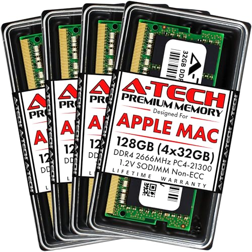
- Very high 128GB capacity in a single four-module kit.
- Designed for specific 27-inch Retina 5K iMac model IDs for better compatibility targeting.
- Runs at standard 1.2V DDR4 voltage.
- Backed by a lifetime warranty and US-based tech support.
Cons
- Compatibility is limited to specific 2019 and 2020 27-inch Retina 5K iMac models.
- Non-ECC unbuffered memory is not suitable for systems that require ECC or registered modules.
- The 128GB capacity may be more than casual users need for everyday tasks.
Overview: The A-Tech 128GB Kit is a four-module DDR4 SO-DIMM upgrade made for compatible 2019 and 2020 27-inch Retina 5K iMac models. The 4 x 32GB layout is aimed at users who want a full-capacity memory upgrade rather than a small bump.
Performance: Running at DDR4 2666 MHz or 2667 MHz and 1.2V, this kit is designed to improve responsiveness, reduce load bottlenecks, and support heavier multitasking. It uses non-ECC, unbuffered, 260-pin SO-DIMM modules with a dual-rank x8 layout.
Drawbacks: Compatibility is limited to iMac19,1, iMac20,1, and iMac20,2 systems, so buyers should confirm the exact model before ordering. The 128GB capacity is also more than many everyday users need, and it will not suit systems that require ECC or registered memory.
Verdict: This kit is best for creators, developers, and professionals who run demanding workloads on supported 27-inch Retina 5K iMacs. For the right machine, it offers a straightforward path to maximum memory capacity with warranty support from A-Tech.
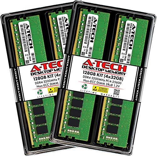
Pros
- Large 128GB capacity is well suited to memory-intensive desktop workloads.
- Standard DDR4 UDIMM form factor makes installation straightforward in compatible computers.
- Clearly rated at 3200MHz, CL22, and 1.2V for easier system matching.
- Backed by a lifetime warranty from A-Tech.
Cons
- Compatibility is limited to select DDR4 desktop systems, so it is not a universal upgrade.
- Non-ECC unbuffered memory is not suitable for systems that require ECC support.
- To use the full 128GB capacity, the motherboard and CPU must support high-density 32GB modules.
Overview: The A-Tech 128GB (4x32GB) DDR4 3200MHz UDIMM kit is a desktop memory upgrade designed for compatible DDR4 systems. Its four-module layout and standard 288-pin UDIMM format make it a straightforward option for supported motherboards.
Performance: With 3200MHz speeds, PC4-25600 ratings, CL22 latency, and a 1.2V JEDEC profile, this kit is built to improve multitasking headroom and help responsive performance in memory-heavy desktop use.
Considerations: The main limitation is compatibility. This is non-ECC, unbuffered desktop RAM, so it is not intended for systems that need server-class ECC memory or other specialized configurations.
Verdict: For users with a compatible DDR4 desktop who need large-capacity memory and prefer a standard, easy-to-install kit, this A-Tech set is a practical choice. It is best for buyers who value capacity and support coverage over niche features.
Reference for Memory Speed Terms
MHz and MT/s are related but not identical units, and mixing them up can make spec sheets look confusing. Checking definitions against a general electronics reference such as American National Standards Institute (ANSI) is a sensible habit before buying.