
Quick Answer
Run Thaiphoon Burner (freeware), click Read u2192 any DIMM slot identifier, and inspect the Die Density/Count field. Cross-reference the SPD manufacturer code against FPSHeaven’s B-Die Finder for pre-purchase lookups. Samsung B-Die, SK Hynix A-Die, and SK Hynix M-Die each carry distinct SPD signatures, voltage ceilings, and overclocking headroom.

Pros
- Rated for speeds up to 6400MT/s with AMD EXPO profile
- Tight CL30-39-39-102 latency timings at 1.40V
- Designed and validated for AMD X870, X670, and B650 platforms
Cons
- Requires manual BIOS overclocking to exceed base JEDEC speeds
- Peak speed depends heavily on motherboard and CPU capability

Pros
- 32GB capacity handles demanding games, multitasking, and creative workloads
- 6000MT/s speed with CL30 latency is well suited for AMD Ryzen performance
- AMD EXPO profiles make enabling rated speeds simple in BIOS
- FURY Beast series is a well known Kingston memory line for desktop builds
Cons
- DDR5 memory requires a DDR5 compatible motherboard, so it will not work with older DDR4 systems
- EXPO is designed for AMD platforms, so Intel users may need to rely on XMP or manual settings
The Kingston FURY Beast 32GB 6000MT/s DDR5 CL30 is best for AMD builders who want high capacity memory with easy overclocking through EXPO profiles. The 6000MT/s speed and CL30 latency pair well with modern Ryzen systems for responsive gaming and multitasking. The main trade-off is that this is DDR5 only, so it requires a compatible DDR5 motherboard and will not fit older DDR4 systems.
Capacity: 32GB
Type: DDR5
Speed: 6000MT/s
Latency: CL30
Overclocking: AMD EXPO
Pros
- Very high 7200MHz DDR5 speed rating for a performance-focused desktop build.
- 32GB capacity in a 2x16GB configuration supports dual-channel operation.
- XMP 3.0 support makes performance tuning more convenient on compatible boards.
- Power management ICs are included for stable and efficient power usage.
Cons
- Requires a compatible 600 or 700 series chipset platform to fully benefit from its rated performance.
- High-speed DDR5 kits like this can be more expensive than lower-frequency alternatives.
- RGB lighting may add value for some users but is unnecessary for buyers focused only on raw performance.
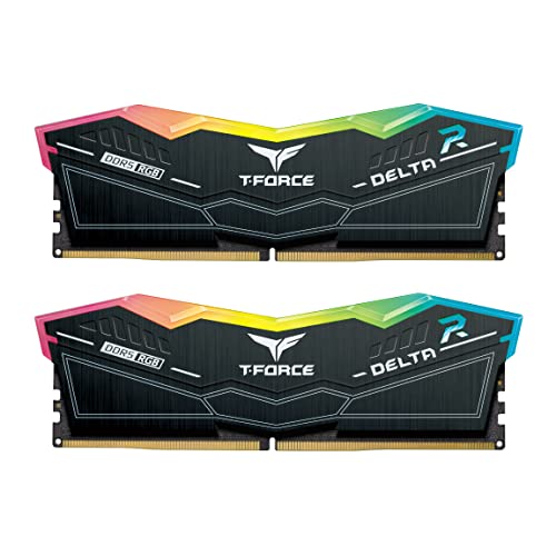
Overview & Design: The TEAMGROUP T-Force Delta RGB DDR5 32GB kit is a desktop memory upgrade built around a 2x16GB layout, 7200MHz speed, and CL34 timings. It is designed for users who want a performance-oriented RAM kit with an RGB look for modern gaming or creator PCs.
Performance & Key Features: Its high frequency, XMP 3.0 readiness, and A-DIE design make it a strong fit for demanding workloads where memory bandwidth matters. The included power management ICs are intended to support stable and efficient power usage, and the kit is aimed at 600 and 700 series chipset systems that can take advantage of fast DDR5 memory.
Drawbacks & Considerations: This is a premium-spec kit, so it is best suited to users with a compatible motherboard and CPU platform. Buyers should also remember that very fast DDR5 can depend heavily on system compatibility, and RGB lighting adds visual appeal rather than direct performance.
Verdict: The T-Force Delta RGB DDR5 32GB 7200MHz CL34 kit makes the most sense for enthusiasts, gamers, and creators building a compatible high-performance desktop. If you want fast DDR5 memory with a polished design and easy profile support, it is a strong option to consider.

Pros
- Fast 6000MHz rated speed with tight CL30-36-36-76 timings
- Ten individually addressable RGB LEDs per module
- Supports AMD EXPO and Intel XMP profiles
- Onboard voltage regulation manageable via CORSAIR iCUE
Cons
- Advertised 6000MHz speed requires manual BIOS overclocking
- Higher 1.77-inch profile may affect compact cooler clearances

Pros
- High 6000MT/s rated speed for a performance-focused DDR5 kit.
- Low CL30 timing is attractive for gamers and PC enthusiasts.
- Works with both Intel XMP 3.0 and AMD EXPO platforms.
- Includes an aluminum heatsink for improved thermal management.
- Backed by a lifetime warranty for long-term ownership confidence.
Cons
- Advertised speeds require compatible motherboard, CPU, and BIOS profile support.
- This is unbuffered UDIMM desktop memory, so it is not intended for laptops or server systems.
- Full performance depends on system configuration, so plug-and-play speeds may run at JEDEC defaults until profiles are enabled.
Overview & Design: The SP Silicon Power Value Gaming DDR5 32GB kit is a desktop memory upgrade made for users who want fast DDR5 performance in a standard 2x16GB UDIMM layout. The aluminum heatsink gives it a practical, heat-conscious design that fits a performance PC build.
Performance & Key Features: Rated at 6000MT/s with CL30 timings and 1.35V operation, this kit is aimed at responsive gaming and demanding multitasking. Support for Intel XMP 3.0 and AMD EXPO makes it easier to run the advertised profile on compatible systems, while the integrated PMIC helps support more stable power delivery.
- 32GB total capacity in a dual-channel 2x16GB kit
- 6000MT/s rated speed with CL30 timing
- XMP 3.0 and AMD EXPO support
- Aluminum heatsink for thermal management
- Lifetime warranty coverage
Drawbacks & Considerations: The main limitation is compatibility, since the advertised speed depends on the motherboard, CPU, and BIOS profile support. As with most high-speed DDR5 kits, plug-and-play behavior may default to JEDEC standards until XMP or EXPO is enabled.
Verdict: This kit makes the most sense for desktop gamers and PC builders who want a fast 32GB DDR5 upgrade with easy profile-based tuning. If your platform supports 6000MT/s DDR5 and you want a balanced mix of speed, cooling, and warranty coverage, it is a strong option to consider.
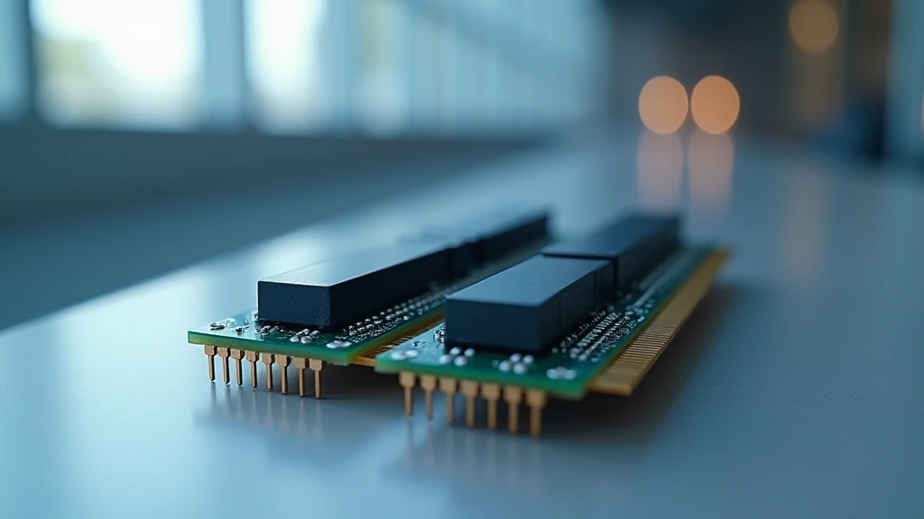
RAM die type is the single most consequential variable in DDR4 and DDR5 overclocking, yet most buyers never look past the marketing sticker on the heat spreader. The silicon die, not the PCB color, not the RGB, not the brand name on the label, determines how far you can tighten primary timings, how high you can push FCLK on Ryzen platforms, and whether your system will run stable at 1.45 V or detonate at 1.40 V. This guide teaches you to identify SK Hynix A-Die, SK Hynix M-Die, and Samsung B-Die with precision, both before and after purchase, using free tools and verifiable part-number databases.
Why RAM Die Type Matters More Than Speed Ratings
A DDR4-3600 CL16 kit built on Samsung B-Die and a DDR4-3600 CL16 kit built on SK Hynix M-Die share identical rated specifications on the retail box, yet their real-world behavior under tight sub-timings diverges dramatically. The die is the physical DRAM chip fabricated on a silicon wafer , the XMP or EXPO profile is merely a factory-tuned operating point written into the SPD EEPROM. Every characteristic that enthusiasts care about , primary timing granularity, tRFC compression, voltage scaling, and thermal headroom , is a function of the die architecture, not the XMP label. For troubleshooting and reliability insights, consult our in-depth set pagefile size windows 11 report.
This distinction becomes critical when pairing memory with a CPU that has a tightly coupled memory controller. When comparing platforms in our AMD Ryzen 5 9600X vs Intel Core Ultra 5 245K analysis, the Ryzen platform’s Infinity Fabric clock ratio means B-Die’s ability to hit DDR4-3800 1:1 FCLK delivers measurable IPC uplift that M-Die at the same speed rating simply cannot replicate due to relaxed tRCD/tRP floors.
The SPD EEPROM: Ground Truth for Die Identification
Every DDR4 and DDR5 module carries a Serial Presence Detect (SPD) EEPROM, a small non-volatile memory chip on the PCB that stores manufacturing data per the JEDEC Memory Standards Specification. Bytes 140 to 145 of the SPD encode the DRAM manufacturer ID (JEP106), the die revision, the die density, and the bank/row/column configuration. Thaiphoon Burner reads these raw bytes and maps them to human-readable strings. No SPD, no identification, physically damaged or counterfeit modules that have had SPD bytes wiped are unidentifiable by software alone.
What the Die Designation Actually Encodes
Samsung uses an internal letter-number suffix on their DRAM part numbers: B-Die refers to the K4A8G085WB-BCPB and related K4Axx variants with the -B revision in the die revision field. SK Hynix’s A-Die maps to H5AN8G8NCJR and similar NCJR-suffixed chips; M-Die maps to NCMM or NDJR suffixes. The letter in the suffix is what Thaiphoon Burner surfaces as the die revision string, which is why reading that field directly from SPD is more reliable than guessing from kit model numbers alone.
Method 1, Thaiphoon Burner (Post-Purchase, Most Accurate)
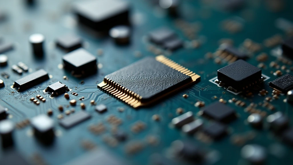
Thaiphoon Burner by Bytemark is the de facto standard SPD decoder for Windows. The freeware version provides full read capability with no feature restriction relevant to die identification. Readers comparing setup options can review our technical analysis on sodimm in desktop pc.
Step-by-Step Procedure
- Download the freeware build from the official Bytemark site (search “Thaiphoon Burner download Bytemark”, avoid third-party mirrors).
- Install and launch with standard user privileges; administrator elevation is not required for read-only SPD access on most Intel and AMD platforms.
- Click the Read tab in the top navigation panel.
- Select any of the presented DIMM slot identifiers, the software auto-enumerates populated slots; selecting any populated slot produces the full SPD dump.
- Locate the Die Density / Count section in the decoded output pane. This field displays the DRAM manufacturer name, the die revision letter, and the per-chip density.
- Cross-reference the DRAM Manufacturer field: “Samsung” with die revision B = Samsung B-Die. “SK Hynix” with die revision A = A-Die; revision M = M-Die; revision C = C-Die.
Interpreting the Output Fields
Beyond the die letter, record three additional values from Thaiphoon Burner for a complete profile: DRAM component part number (the raw chip PN string before Thaiphoon decodes it), module organization (x8 vs x16 chip width, x8 is universally preferred for overclocking), and nominal voltage (1.20 V nominal for standard DDR4). A Samsung B-Die 16 GB stick built with x8 organization at 1.20 V nominal has substantially more voltage headroom to 1.45 V than an x16-organized M-Die stick where the per-die power density is already higher at stock.
Method 2, FPSHeaven B-Die Finder (Pre-Purchase Research)
FPSHeaven’s B-Die Finder indexes over 1,000 verified DDR4 kit configurations by retail part number, cross-mapped to confirmed die type from community SPD reads. This is the correct tool to use before purchasing a kit , particularly for Ryzen 5000 and Intel 12th, 14th gen builds where B-Die at DDR4-3600 to 4000 yields tangible latency benefits. For complementary field maintenance guidelines, examine our breakdown of running out of ram pagefile.
How to Use FPSHeaven’s Database
- Navigate to fpsheaven.com and open the B-Die Finder tool.
- Enter the exact retail part number (e.g., F4-3600C18Q-32GTZN for G.Skill Trident Z Neo 32 GB DDR4-3600 CL18 quad-kit).
- The result returns confirmed die type, kit revision if multiple die revisions shipped under the same SKU, and community verification count.
- If the result returns “M-Die” or “A-Die” for a kit you expected to be B-Die, verify whether a newer PCB revision exists under a different sub-SKU suffix, G.Skill and Corsair both revise die sourcing without changing the primary model number.
The Revision Sub-Suffix Problem
This is the most common source of confusion: identical model numbers (same EAN, same retail listing) can ship with different dies depending on manufacturing batch and quarter. G.Skill’s Trident Z Neo F4-3600C16D-32GTZNC shipped Samsung B-Die through early 2022, then transitioned to SK Hynix A-Die on subsequent batches. The FPSHeaven database tracks these transitions by sub-revision. When the database shows multiple die entries for one SKU, purchase from retailers that display the manufacturing date code or contact the vendor for the current batch die sourcing before committing funds.
Die-by-Die Technical Comparison: B-Die vs A-Die vs M-Die
| Property | Samsung B-Die | SK Hynix A-Die | SK Hynix M-Die |
|---|---|---|---|
| Process Node | 10 nm class (1y) | 10 nm class (1y/1z) | 10 nm class (1z) |
| Chip Organization | x8 (8 Gb per die) | x8 (8 Gb per die) | x8 / x16 (16 Gb per die) |
| Safe Vdimm Ceiling | 1.50 V (daily 1.45 V) | 1.45 V (daily 1.40 V) | 1.40 V (daily 1.35 V) |
| Typical tCL Floor (DDR4-3600) | CL14 to 15 | CL15 to 16 | CL16 to 18 |
| tRFC Compression Potential | Excellent (260 to 280 ns) | Good (300 to 320 ns) | Moderate (340 to 360 ns) |
| Max Stable Frequency (typical) | DDR4-4000 to 4400+ | DDR4-3800 to 4000 | DDR4-3600 to 3800 |
| Thermal Operating Range | 0 to 85 °C | 0 to 85 °C | 0 to 85 °C |
| Overclocking Tier | S-Tier (king of DDR4 OC) | A-Tier (strong mid-range OC) | B-Tier (XMP-only practical) |
| Availability (2025 to 2026) | Scarce, premium priced | Widely available | Dominant in budget kits |
| DDR5 Successor Die | Samsung C-Die (DDR5) | SK Hynix A-Die DDR5 | SK Hynix M-Die DDR5 |
Platform-Specific Considerations for pc hardware 2026
Die type relevance scales with platform memory controller sensitivity. Intel’s Arrow Lake and Lunar Lake IMC tolerates a wider range of dies at high frequency, you can hit DDR5-7200 on mediocre Hynix M-Die with relaxed secondaries and still close the latency gap substantially. AMD’s Zen 5 Infinity Fabric, by contrast, rewards die quality more aggressively: tight secondaries enabled by B-Die (or DDR5 A-Die equivalent) on FCLK 1:1 ratio deliver latency improvements that scale through the entire CPU-to-cache hierarchy. Board firmware also matters, the ASUS ROG Maximus Z890 Hero vs MSI MEG Z890 ACE platforms differ in how aggressively their auto-OC algorithms push secondary timings based on detected die type, with the ROG Maximus applying tighter tRFC automatically when it detects B-Die via SPD.
For DDR5 builds launching in the pc hardware 2026 window, the identification methodology is identical, Thaiphoon Burner reads DDR5 SPD via the new TS5 (Temperature Sensor 5) extended byte map, but the competitive die landscape shifts: Micron B-Die (DDR5) and SK Hynix A-Die DDR5 have largely closed the gap that Samsung B-Die held uncontested through the DDR4 era. GPU memory bandwidth is a separate subsystem, see our Radeon RX 9060 XT 8GB vs 16GB comparison for how GDDR6 capacity affects compute-limited workloads independently of system RAM die type.
Dual-Rank vs Single-Rank Die Organization
Die type interacts with rank configuration. A 16 GB DDR4 stick built with Samsung B-Die in dual-rank x8 configuration (two ranks of eight x8 chips) hits higher stable frequencies than a 32 GB stick with the same die in dual-rank due to increased capacitive load on the trace. When running four DIMMs on a two-channel board, a common scenario for workstation builds, B-Die’s superior signal integrity margin is the reason it tolerates quad-populated slots at DDR4-3600 where M-Die drops to 3200 for stability. Our desktop CPU benchmarks & reviews consistently show 3 to 7% latency improvement in memory-sensitive workloads when moving from XMP-only M-Die to B-Die with tight secondaries on the same platform.
Reading the DRAM Chip Markings Directly (Hardware Method)
When SPD is inaccessible, corrupted EEPROM, dead system that won’t POST, or a bare die without a PCB, the physical chip markings on the DRAM ICs are the fallback. Remove the heat spreader (voids warranty on most kits) and read the laser-etched part number on each black DRAM chip.
Samsung B-Die Chip Marking Pattern
Samsung DDR4 B-Die chips carry part numbers beginning with K4A8G085WB (8 Gb density) or K4AAG085WB (16 Gb, dual-die package). The critical character is the second letter after the dash: -BCPB, -BCTD, -BCWD, the leading B identifies the die revision. Any Samsung DDR4 chip whose suffix begins with -B is B-Die.
SK Hynix A-Die and M-Die Chip Marking Pattern
SK Hynix DDR4 chip part numbers follow the pattern H5AN8G8NCJR (A-Die, x8, 8 Gb) and H5AN8G8NCMR or H5ANAG8NCMR (M-Die, higher density). The third-to-last letter in the suffix encodes the die revision: C = A-Die (confusingly, Hynix’s internal revision letter for A-Die is C in the part number), M = M-Die. SK Hynix’s naming convention is orthogonal to Samsung’s, do not conflate the part number die letter with the marketing die name.
For GPU-adjacent research comparing how memory subsystem choices affect rendering throughput, the graphics card tests & GPU guides section covers VRAM architecture decisions that parallel the system RAM die-type tradeoffs discussed here.
Final Diagnostic Verdict & Maintenance Checklist
Die type identification is a three-minute procedure with Thaiphoon Burner and a non-negotiable step before any overclocking attempt. Running voltage beyond the safe ceiling for your specific die, particularly pushing M-Die past 1.40 V or A-Die past 1.45 V, risks accelerated electromigration in the die interconnects, manifesting initially as increased bit-error rate under stress and eventually as permanent cell failure. The damage is cumulative and non-reversible.
Pre-Purchase Checklist
- Search the exact retail SKU on FPSHeaven B-Die Finder before ordering.
- If multiple die types are listed for one SKU, contact the vendor for current batch sourcing or buy from a retailer who displays the batch date code.
- Prioritize x8 chip organization over x16 for overclocking, verify this in the product datasheet or ask the vendor; it is rarely printed on retail packaging.
- Factor in platform: B-Die premium is most justified on Ryzen 5000/7000 and Intel 12th-14th gen; less justified on platforms with a weak IMC that cannot leverage tight secondaries regardless of die quality.
Post-Installation Checklist
- Run Thaiphoon Burner immediately after first boot, confirm die type, die revision letter, chip organization, and nominal voltage before enabling XMP/EXPO.
- Set Vdimm to no more than 0.10 V above nominal (1.20 V + 0.10 V = 1.30 V as a safe XMP baseline) before pushing higher incrementally.
- Validate stability with at least two passes of MemTest86 6.0+ at the target frequency before tightening any secondary timings.
- Monitor DIMM temperature under full memory bandwidth load, target below 50 °C on the SPD temperature sensor; above 60 °C under sustained load indicates inadequate airflow and will degrade die longevity regardless of voltage.
- Re-read SPD with Thaiphoon Burner after any BIOS update, some board firmware updates reset DRAM training data and may expose a timing incompatibility with a marginal die that was previously masked by training cache.
- Document the full Thaiphoon Burner output (screenshot or export), this is the authoritative record for RMA and warranty claims if the kit fails under a disputed overclocking condition.
Samsung B-Die remains the gold standard for DDR4 overclocking in 2025 to 2026, but its scarcity means SK Hynix A-Die is the realistic top-tier option for most new builds. M-Die is competent at rated XMP speeds and requires no apology in a system that will never see manual OC. The methodology above, SPD via Thaiphoon Burner, pre-purchase via FPSHeaven, physical markings as last resort, covers every identification scenario with no ambiguity, no guesswork, and no reliance on the heat spreader label that tells you nothing about the silicon underneath it.
Pointers for Module Identification
Reading module labels and die markings takes patience, and a guide on desktop pcs may give broader context for the system around them. Background on electronics identification terms is found at American National Standards Institute (ANSI).