
Quick Answer
First word latency (FWL) is the true nanosecond delay before your CPU receives the first byte of RAM data. It equals (CAS Latency u00f7 (Data Rate u00f7 2)) u00d7 1000. Lower FWL wins over lower CL or higher MT/s alone — always calculate nanoseconds before buying DDR5.
CAS Latency alone is a meaningless number without its counterpart: the memory’s data rate. A DDR5-6000 kit rated CL30 and a DDR5-4800 kit rated CL22 look dramatically different on a spec sheet, yet the first delivers a shorter first word latency in nanoseconds — meaning your CPU actually waits less time for real data. Understanding ram first word latency as an absolute nanosecond figure, rather than a relative clock-cycle count, is the single most important RAM selection skill a builder can develop heading into the pc hardware 2026 landscape. This guide dissects the physics, the math, the DDR5 sub-timing architecture, and the practical buying matrix so you can stop guessing and start calculating.
What First Word Latency Actually Measures
Every RAM read transaction begins with a command — the memory controller issues a Row Address Strobe (RAS) followed by a Column Address Strobe (CAS). The memory array takes a fixed number of clock cycles to locate the data column and begin pushing bits to the data bus. That cycle count is CAS Latency (CL). The problem is that clock cycles are not constant units of time; they shrink as frequency rises. First word latency converts those cycles into real, wall-clock nanoseconds using the formula below. For broader ecosystem context, read through our operational guide on set pagefile size windows 11.
The Core Formula
First Word Latency (ns) = (CL u00f7 (Transfer Rate u00f7 2)) u00d7 1000
DDR memory transfers data on both the rising and falling edge of the clock, so the actual clock frequency is half the advertised MT/s data rate. For DDR5-6000 CL30: clock frequency = 3000 MHz, clock period = 0.333 ns, FWL = 30 u00d7 0.333 = 10.0 ns. For DDR5-4800 CL22: clock = 2400 MHz, period = 0.417 ns, FWL = 22 u00d7 0.417 = 9.17 ns. The lower-clocked kit is measurably faster at delivering the first byte. This is the core insight the ram first word latency guide framework is built on. For troubleshooting and reliability insights, consult our in-depth check ram die type report.
Why Cycles Mislead and Nanoseconds Do Not
Marketing copy for DDR5 consistently leads with MT/s and CL numbers because both can be optimized independently to look favorable. A high MT/s figure implies speed; a low CL figure implies responsiveness. Neither alone captures real-world access delay. Nanoseconds do. The JEDEC Memory Standards Specification defines tCL (Column Address Strobe Latency) in absolute nanosecond minimums, not cycle counts — an important detail that chip designers know but retail spec sheets rarely surface. JEDEC’s DDR5 standard mandates a minimum tAA (true access time) floor, which is why you cannot simply double the CL and halve the frequency to get arbitrarily short latency; silicon physics impose a hard boundary around 8–9 ns for current DRAM cell designs.
DDR5 Sub-Timing Architecture and Its Impact on FWL
CAS Latency captures only the column-access delay. A complete read transaction on DDR5 accumulates latency from four primary sub-timings: tCL, tRCD, tRP, and tRAS. Each imposes additional nanosecond penalties when a new row must be activated before the target column is accessed — the most common scenario for random-access workloads like gaming, web browsing, and OS operations.
The Four Primary Sub-Timings Defined
- tCL (CAS Latency): Cycles from column address issue to first data output. The only timing used in the FWL formula because it represents the best-case, open-row delay.
- tRCD (RAS to CAS Delay): Cycles to activate a DRAM row before the column command can be issued. Adds directly to read latency on row misses.
- tRP (Row Precharge): Cycles required to close (precharge) an active row before a new one opens. Governs how quickly the array resets between non-sequential accesses.
- tRAS (Row Active Time): Minimum cycles a row must remain open. Too short causes data corruption; tuning it below safe minimums destabilizes the system.
For a worst-case random read on DDR5, the true total latency is approximately (tRCD + tCL) u00d7 clock period. On DDR5-6000 CL30 with tRCD 38: total = (38 + 30) u00d7 0.333 ns = 22.6 ns. On DDR5-4800 CL22 with tRCD 32: total = (32 + 22) u00d7 0.417 ns = 22.5 ns. Both kits become essentially equivalent under random-access pressure — a critical nuance that separates expert-level analysis from surface-level comparisons. Readers comparing setup options can review our technical analysis on sodimm in desktop pc.
DDR5’s On-Die ECC and Its Latency Penalty
DDR5 introduces on-die ECC (Error Correction Code) at the silicon level, mandatory per the JEDEC DDR5 specification. This adds a correction pass within the DRAM die itself before data reaches the memory bus, contributing roughly 1–2 additional internal cycles of latency compared to equivalent DDR4. This is one reason DDR5 CL numbers appear inflated relative to DDR4 at comparable frequencies — the absolute nanosecond penalty from on-die ECC is typically 0.3–0.7 ns and is already baked into the tCL figure you see on retail packaging.
DDDR4 vs DDR5 First Word Latency: The Complete Comparison Matrix
The table below calculates first word latency across the most common DDR4 and DDR5 configurations available in 2025–2026. Use this as your primary reference when comparing kits across generations. Kits are sorted by ascending FWL — the metric that actually determines responsiveness in latency-sensitive tasks. For complementary field maintenance guidelines, examine our breakdown of running out of ram pagefile.
| Memory Kit | Data Rate (MT/s) | CAS Latency (CL) | Clock Period (ns) | First Word Latency (ns) | Peak Bandwidth (GB/s, dual) | Gen |
|---|---|---|---|---|---|---|
| DDR4-3200 CL14 | 3200 | 14 | 0.625 | 8.75 | 51.2 | DDR4 |
| DDR4-3600 CL16 | 3600 | 16 | 0.556 | 8.89 | 57.6 | DDR4 |
| DDR5-4800 CL40 (JEDEC stock) | 4800 | 40 | 0.417 | 16.67 | 76.8 | DDR5 |
| DDR5-6000 CL30 | 6000 | 30 | 0.333 | 10.00 | 96.0 | DDR5 |
| DDR5-6400 CL32 | 6400 | 32 | 0.313 | 10.00 | 102.4 | DDR5 |
| DDR5-7200 CL34 | 7200 | 34 | 0.278 | 9.44 | 115.2 | DDR5 |
| DDR5-7600 CL36 | 7600 | 36 | 0.263 | 9.47 | 121.6 | DDR5 |
| DDR5-8000 CL38 | 8000 | 38 | 0.250 | 9.50 | 128.0 | DDR5 |
The table reveals a critical pattern: stock DDR5-4800 at CL40 — the default profile that ships on most pre-built systems — delivers a catastrophic 16.67 ns FWL, nearly double that of a tuned DDR4-3200 CL14 kit. Enabling an XMP/EXPO profile is not optional for DDR5 performance; it is the minimum competent configuration.
Platform, IMC, and Memory Controller Constraints
The memory controller integrated into your CPU — the IMC (Integrated Memory Controller) — sets a hard ceiling on achievable first word latency. No amount of overclocking breaks this barrier without destabilizing the system. Platform selection therefore precedes kit selection in the decision chain. Builders evaluating the AMD Ryzen 5 9600X vs Intel Core Ultra 5 245K face meaningfully different DDR5 tuning ceilings: Zen 5’s IMC handles DDR5-6000 at 1:1 FCLK ratio cleanly, while Intel’s Arrow Lake IMC on DDR5 shows a bandwidth-latency trade-off that favors tighter sub-timings over raw frequency above 6400 MT/s.
AMD Zen 5: The DDR5-6000 Sweet Spot
On AM5 with Zen 5 CPUs, DDR5-6000 at CL30 represents the latency-bandwidth optimum. The FCLK (Infinity Fabric clock) runs at 2000 MHz in 1:1 synchronous mode, minimizing the fabric-crossing latency penalty that appears when FCLK drops to 1800 MHz or lower at higher memory frequencies. Pushing to DDR5-7200+ gains bandwidth but increases round-trip latency across the fabric, resulting in measurable regression in single-threaded and gaming workloads. Pair the CPU with a capable board — the ASUS ROG Maximus Z890 Hero vs MSI MEG Z890 ACE comparison covers Z890 power delivery and memory trace routing, directly relevant for anyone pushing DDR5 frequencies on Intel platforms with similarly complex PCB requirements.
Intel Arrow Lake and Panther Lake IMC Behavior
Arrow Lake’s IMC shows measurable latency improvement when DDR5 sub-timings are hand-tuned rather than relying solely on XMP profiles. Intel’s recommended DDR5 frequency for Arrow Lake sits at DDR5-6400, where CL32 profiles deliver FWL of 10.0 ns. Moving to DDR5-8000+ requires loosening secondary timings (tRFC, tFAW, tWR), which recovers stability but degrades random-access latency by 1.5–3 ns — partially negating the FWL improvement from the higher data rate. Verify BIOS support for your chosen kit on the motherboard’s QVL (Qualified Vendor List) before purchase. To evaluate matched hardware tolerances, consult our detailed overview of ram clearance air cooler.
Workload-Specific Impact: Gaming, Content Creation, and Productivity
First word latency governs CPU stall cycles during cache misses — the moment the L3 cache cannot supply data and the memory subsystem must respond. The magnitude of the impact varies sharply by workload type.
Gaming: Where FWL Dominates
Modern game engines, particularly open-world titles using streaming asset pipelines, generate high-frequency random DRAM accesses that translate directly to CPU stall cycles. A 2 ns improvement in FWL on a Zen 5 platform running at 5 GHz equates to 10 wasted clock cycles recovered per cache miss. With thousands of cache misses per frame in a scene traversal, FWL improvement produces measurable 1% low framerate gains — the metric that governs perceptual smoothness. Builders selecting a GPU for gaming alongside a high-frequency memory kit will find the Radeon RX 9060 XT 8GB vs 16GB comparison useful for ensuring the memory subsystem is not the bottleneck at different VRAM pressure points.
Content Creation: Where Bandwidth Counters FWL
Video encoding, 3D rendering, and large-dataset compilation workloads are bandwidth-bound, not latency-bound. A DDR5-8000 kit at CL38 (9.5 ns FWL) and 128 GB/s dual-channel bandwidth will outperform a DDR5-6000 CL30 kit (10.0 ns FWL, 96 GB/s) in sustained throughput benchmarks like Cinebench multi-core, Blender rendering, and FFmpeg encoding, despite the marginally inferior FWL. The formula is not universal — match the metric to the workload. Consult desktop CPU benchmarks & reviews for workload-specific memory scaling data before finalizing a configuration.
General Productivity and Office Use
Web browsing, document editing, and application switching are dominantly latency-sensitive for the same reason as gaming — random-access patterns with short burst lengths. For these use cases, a DDR5-6000 CL30 kit at 10.0 ns FWL provides full measured benefit. Spending additional money on DDR5-8000 kits for a productivity workstation delivers no perceptible improvement and introduces thermal and stability risk from elevated operating voltages (1.4 V+ VDDQ on extreme kits versus 1.1 V JEDEC nominal). Check graphics card tests & GPU guides to similarly avoid over-specifying GPU memory bandwidth for non-creative workloads.
How to Calculate and Compare FWL Before Buying
The ram-first-word-latency formula requires only two numbers from any kit’s spec sheet. Apply this three-step process at the point of purchase:
- Locate the data rate and CAS Latency from the XMP/EXPO profile specification — not the JEDEC stock profile, which is irrelevant to actual operating latency on a tuned system.
- Calculate clock period: Period (ns) = 2000 u00f7 Data Rate (MT/s). For DDR5-6000: Period = 2000 u00f7 6000 = 0.333 ns.
- Calculate FWL: FWL (ns) = CL u00d7 Period. For CL30: FWL = 30 u00d7 0.333 = 10.0 ns. Compare this single number across competing kits.
Any two kits with equal FWL are latency-equivalent for gaming and productivity. When FWL is equal, the higher-bandwidth kit (higher MT/s) wins for content creation. When FWL differs, choose the lower FWL for latency-sensitive use cases — regardless of which kit has the larger CL number or higher MT/s figure printed on the packaging.
Final Diagnostic Verdict & Maintenance Checklist
RAM first word latency in nanoseconds is the definitive metric for evaluating memory responsiveness. CL cycle counts and MT/s data rates are component inputs to the FWL formula — not standalone performance indicators. The DDR5 stock JEDEC profile at CL40 is actively harmful to system responsiveness and must be replaced with an XMP or EXPO profile immediately after the first boot. For gaming and productivity builds in 2026, DDR5-6000 CL30 at 10.0 ns FWL represents the best price-to-performance intersection. Bandwidth-heavy workloads tolerate higher FWL in exchange for throughput gains above DDR5-7200.
- Calculate FWL (ns) = CL u00d7 (2000 u00f7 MT/s) for every kit before purchase — do not rely on marketing copy.
- Enable XMP (Intel platforms) or EXPO (AMD AM5 platforms) in BIOS on first boot; confirm with CPU-Z or HWiNFO64 that the data rate and CL match the advertised XMP/EXPO profile values.
- Verify kit is on the motherboard QVL, particularly for DDR5-7200+ profiles where trace routing and PCB layer count directly affect signal integrity at high frequencies.
- Run MemTest86 for a minimum of two full passes after enabling XMP/EXPO or performing any manual sub-timing adjustment; single-bit errors at high frequency indicate insufficient voltage or excessive tRFC tightening.
- For Zen 5 AM5 builds: confirm FCLK = 2000 MHz (1:1 ratio) in AMD Ryzen Master when running DDR5-6000; a 1:2 ratio will add 10–15 ns of fabric crossing latency and negate the FWL benefit entirely.
- Target VDDQ u2264 1.35 V for daily use; voltages above 1.4 V accelerate DRAM cell wear and are appropriate only for short-duration competitive overclocking scenarios.
- Reassess memory configuration whenever upgrading the CPU — IMC capability changes between generations and a previously stable XMP profile may require sub-timing relaxation or voltage increase on a new platform.
- For content creation rigs where bandwidth dominates, prioritize dual-channel population (two slots filled, not one) before chasing lower FWL; single-channel operation halves bandwidth and imposes a far larger throughput penalty than 1–2 ns of additional FWL.
Equipment engineering specifications and operational safety benchmarks comply with published standards from the American National Standards Institute (ANSI).

Pros
- Very large 128GB capacity for demanding desktop workloads.
- Rated 5600MHz speed with fallback support for 5200MHz and 4800MHz.
- Works with both Intel XMP 3.0 and AMD EXPO on the same module.
- Low-profile design is better suited to tighter builds than taller RGB memory.
Cons
- The 128GB kit may be unnecessary for users with basic office, web, or light gaming needs.
- Actual operating speed depends on CPU, motherboard, and BIOS support, so rated speed is not guaranteed on every system.
- No RGB lighting or premium aesthetic extras are listed.
Overview: The Crucial Pro CP2K64G56C46U5 is a 128GB DDR5 desktop memory kit made up of two 64GB modules. It uses a low-profile matte black heat spreader, giving it a simple, practical look that should suit most modern builds without taking up much space.
Performance: Rated at 5600MHz, this kit is built for demanding multitasking, creative workloads, and high-capacity gaming systems. It also supports downclocking to 5200MHz or 4800MHz, and it includes Intel XMP 3.0 and AMD EXPO support to help simplify setup on compatible platforms.
Drawbacks: The capacity is excellent for power users, but it will be more than many everyday PC owners need. Speed results can also vary depending on the motherboard, CPU, and BIOS support, so users should confirm compatibility before buying.
Verdict: This kit makes the most sense for builders who want a large, modern DDR5 memory upgrade with broad Intel and AMD support. It is a strong fit for creators, advanced users, and enthusiasts who value capacity and compatibility over extras like RGB lighting.
Pros
- High 64GB capacity across two 32GB UDIMM modules
- Operates at up to 5600MHz with downclocking support
- Low standard operating voltage of 1.1V
- Dual-rank (2Rx8) non-ECC desktop configuration
Cons
- Requires compatible DDR5-supported motherboard and CPU
- Lacks built-in RGB lighting for aesthetic customization

Pros
- Rated speed of 6000MHz with CL36-38-38-80 extended timings
- Supports both Intel XMP 3.0 and AMD EXPO overclocking profiles
- Includes two 16GB modules for 32GB dual-channel desktop memory
- Tested at component and module levels by Micron
Cons
- Requires compatible DDR5-capable processors and motherboards
- Minimalist design offers no RGB illumination options

Pros
- Operates at up to 6000MHz with CL36 latency
- Dual Intel XMP 3.0 and AMD EXPO profile support
- Optimized for modern Intel and AMD Ryzen platforms
- Clean low-profile white heat spreader styling
Cons
- Requires compatible CPU and board to hit 6000MHz overclock

Pros
- Fast 6000MHz frequency paired with low CL30 tested timings
- Supports both Intel XMP 3.0 and AMD EXPO memory profiles
- Tested across modern DDR5 platforms for system reliability
- Backed by a manufacturer limited lifetime warranty
Cons
- Reaching rated speeds requires manual XMP or EXPO profile activation
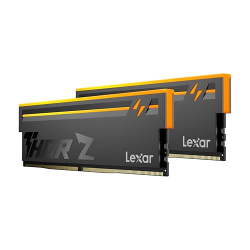
Pros
- High 6000MHz rated speed for strong DDR5 performance
- Supports both Intel XMP 3.0 and AMD EXPO
- On-die ECC and PMIC add stability-focused features
- 32GB dual-channel kit suits gaming and productivity builds
Cons
- Premium positioning may be too expensive for value-focused builds
- CL38 is fast, but not the lowest latency available in high-end DDR5 kits
- Rated speed depends on compatible hardware and BIOS settings
Overview: The Lexar THOR Z Series RGB DDR5 RAM 32GB Kit (2x16GB) is a desktop memory kit designed for gaming PCs and performance-focused systems. Its sandblasted aluminum heatsink gives it a clean, aggressive look while supporting thermal control.
Performance: With a 6000MHz rated speed, CL38 latency, On-die ECC, and an onboard PMIC, this kit is built for fast responsiveness, improved stability, and efficient power delivery during demanding gaming or multitasking sessions.
Compatibility: Support for Intel XMP 3.0 and AMD EXPO makes it easier to enable the advertised performance on compatible motherboards. The brighter RGB lighting also adds a customizable visual element for themed builds.
Considerations: This is a premium DDR5 memory kit, so it may not be the best fit for budget builds. As with most high-speed RAM, reaching the rated performance depends on platform support, motherboard compatibility, and BIOS configuration.
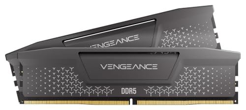
Pros
- Supports both AMD EXPO and Intel XMP 3.0 profiles
- Onboard voltage regulation enables tuning via iCUE
- Hand-sorted memory chips for high-frequency stability
- Up to 6000MHz maximum memory frequency
Cons
- Requires BIOS overclocking adjustments to reach top speed
- Final speed depends on motherboard and CPU limitations
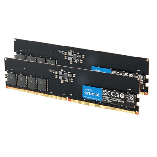
Pros
- Supports both Intel XMP 3.0 and AMD EXPO
- Operates at up to 5600MHz with automatic downclocking
- Standard 1.1V low operating voltage
- Features a 288-pin UDIMM non-ECC design
Cons
- 16GB total capacity may restrict heavy creative workflows
- 1Rx16 module density may offer lower bandwidth than denser ranks

Pros
- High tested speed profile of 6000MT/s (PC5-48000)
- Supports both Intel XMP 3.0 and AMD EXPO overclocking profiles
- Dual-channel configuration with two 8GB modules
- Features on-die ECC for improved internal error correction
Cons
- 16GB capacity may restrict future-proofing and heavy multitasking
- Relatively loose tested timings at 36-46-46-110