
Quick Answer: Ddr5 Voltage Vdive Vpp Safe Limits Overview
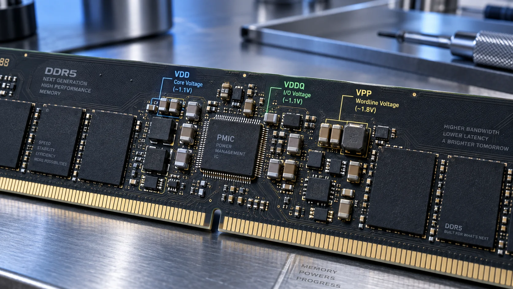
DDR4 used a single primary voltage domain, 1.2 V nominal for both core logic and I/O, with a separate 2.5 V VPP rail for the self-refresh capacitor charge pump. DDR5 splits core logic and I/O into two separately regulated rails, collapses the nominal from 1.2 V to 1.1 V, and retains VPP at 1.8 V. This is not a cosmetic change. The split VDD/VDDQ architecture is required because DDR5 integrates a Power Management IC (PMIC) directly on the DIMM itself, replacing the motherboard-side voltage regulator that handled DDR4 supply rails.
That on-module PMIC accepts a single 5 V or 12 V input from the motherboard and internally generates all three rails with tight per-module regulation. The result is tighter voltage tolerance windows, better noise immunity on high-frequency signal traces, and less board-layer complexity for motherboard OEMs, but it also means voltage manipulation for overclocking now happens at the PMIC level, either via BIOS tuning of PMIC target codes or, in some extreme XMP/EXPO scenarios, via direct register writes. Understanding what each rail does, and what pushing it costs, is prerequisite knowledge before touching any BIOS voltage slider.
Platform context matters here too. Just as you would consult data on CPU temperature limits before sustained gaming loads, RAM voltage ceilings must be understood in relation to both the JEDEC specification and your specific IC silicon quality before any manual tuning begins.
DDR5 Voltage Rails: Specifications, Safe Limits, and Degradation Thresholds
| Rail | Function | JEDEC Nominal | JEDEC Max (Abs.) | Safe Daily OC Ceiling | Degradation Risk Zone | Notes |
|---|---|---|---|---|---|---|
| VDD | Core array logic, sense amplifiers, internal clocks | 1.1 V | 1.5 V | u2264 1.35 V (24/7) | > 1.40 V | Tied to VDDQ in most PMIC implementations; raising one raises both |
| VDDQ | DQ I/O drivers, data bus termination, ODT | 1.1 V | 1.5 V | u2264 1.35 V (24/7) | > 1.40 V | Higher VDDQ improves signal integrity at elevated data rates; overdriving stresses I/O cells |
| VPP | Capacitor plate charge pump, row activation (ACT) energy | 1.8 V | 2.0 V | u2264 1.9 V (24/7) | > 1.95 V | Impacts tRCD/tRAS timing margins; excess VPP accelerates gate oxide wear in charge pump circuitry |
| VDDQ_TX | Transmit I/O sub-rail (some PMIC implementations) | 1.1 V | 1.5 V | Matches VDDQ | Follows VDDQ threshold | Transparent to end user; regulated by PMIC automatically |
| VDD2H (Host-side) | Memory controller I/O on CPU/SoC die | Platform-defined (typically 1.1 V) | Platform BIOS-defined | u2264 1.25 V | > 1.3 V | Intel calls this VDDMC; AMD labels it SOC voltage or VDDIO_MEM; raising this helps controller stability at high frequencies |
VDD and VDDQ: Why They Travel Together and What That Means for Overclocking
In the DDR5 specification, VDD powers the core memory array and all internal logic , sense amplifiers, row decoders, refresh control circuits, and the mode register set. VDDQ powers the data I/O interface: the DQ and DQS drivers that physically push signal onto the memory bus. In theory these are independent rails. In practice, the vast majority of current PMIC designs , including those from Montage Technology, Richtek, and MPS , tie their target regulation codes together. When your BIOS presents a single “DRAM Voltage” slider, it adjusts both VDD and VDDQ simultaneously through the same PMIC command sequence. For troubleshooting and reliability insights, consult our in-depth what power supply wattage for gaming pc report.
This coupling matters for overclocking logic. Raising DRAM voltage to 1.35 V to stabilize DDR5-7200 means both the core array and the I/O cells are seeing that elevated supply. Higher VDD provides more margin to sense amplifiers during fast CAS operations. Higher VDDQ reduces signal integrity issues by boosting driver swing, which is especially significant on longer trace boards or dual-DIMM configurations where stub reflections are harder to control. The downside is compounded thermal stress: both domains heat up together, and I/O cells in deep-submicron nodes are particularly sensitive to sustained elevated voltage combined with elevated temperature.
Safe daily ceiling consensus among experienced overclockers and validated by silicon vendor thermal-aging data sits at 1.35 V for 24/7 operation. Pushing to 1.40 V for benching sessions is documented as achievable but should not be run continuously. Above 1.40 V, hot carrier injection (HCI) effects and time-dependent dielectric breakdown (TDDB) in the array transistors accelerate measurably, the same physical mechanisms that govern thermal paste application discipline on the CPU die apply as system-level thermal management principles here: heat and voltage stress compound multiplicatively, not additively.
VPP: The Most Misunderstood DDR5 Rail
VPP is the charge pump supply that energizes the capacitor plates inside each DRAM cell during row activation (ACT) and precharge (PRE) operations. In DDR4, VPP ran at 2.5 V. DDR5 drops this to 1.8 V , a significant process node improvement that reduces activation energy requirements while maintaining sufficient charge to flip cell states reliably at DDR5-class refresh rates and tighter timing targets. Readers comparing setup options can review our technical analysis on how to fix intel arrow lake z890 bios voltage.
VPP does not directly affect data bus signal quality. Its primary influence is on row-hammer mitigation circuitry (PRAC, RFM commands in DDR5), refresh timing parameters (tRFC, tREFI), and the energy available for row activation, which translates to tRCD and tRAS timing margins. When overclockers tighten tRCD aggressively and hit instability, a modest VPP bump from 1.8 V to 1.85 to 1.9 V is often the correct lever because it restores charge pump energy headroom, not because it affects the data path.
JEDEC absolute maximum for VPP is 2.0 V. Field-tested safe daily ceiling is 1.9 V. Beyond 1.95 V, wear in the charge pump’s switched-capacitor network accelerates in a manner analogous to electromigration in power delivery traces: individually imperceptible, cumulatively fatal over months. Note that some motherboard BIOS implementations expose VPP as an independent slider; others lock it to a fixed offset above VDD. Check your UEFI documentation , incorrectly tuned VPP can cause correctable error (CE) rate spikes that appear as random application crashes rather than clean boot failures, making diagnosis harder. For complementary field maintenance guidelines, examine our breakdown of how to safely connect 12v 2×6 gpu power cable.
Platform-Specific Voltage Behavior: Intel vs. AMD DDR5
Intel Alder Lake / Raptor Lake / Arrow Lake (LGA1700 / LGA1851)
Intel’s memory controller communicates with the PMIC via the SPD Hub (SPD5118 or equivalent) over an I3C bus. BIOS voltage adjustments write target codes to the PMIC, which regulates the actual output. Intel platforms expose VDD/VDDQ as a unified “DRAM Voltage” field and a separate VPP field. The host-side controller rail, labeled VDDMC or internally as VDD2H, is adjustable via the “Memory Controller Voltage” or “System Agent Core Voltage” slider depending on BIOS vendor implementation. Raising VDDMC to 1.15 to 1.2 V is standard practice for DDR5-6400 and above on Intel platforms. Intel’s official DDR5 specification documentation is published at intel.com’s DDR5 memory resource hub and details the supported voltage ranges per platform.
AMD Ryzen 7000 / 9000 Series (AM5)
AMD’s AM5 platform uses a unified Infinity Fabric and memory controller subsystem where VDDIO_MEM (the host-side DDR5 I/O supply on the SoC die) is distinct from the DRAM module voltage. AMD EXPO profiles bake specific VDD/VDDQ and VPP values into the SPD profile, which the PMIC applies on XMP/EXPO enable. AMD’s memory controller is generally considered to offer slightly more headroom at high frequencies on AM5 than Raptor Lake did on LGA1700, but it is also more sensitive to SOC voltage (VSOC) stability, underpowering VSOC while overvolting DRAM is a common source of intermittent training failures on AM5. Understanding how PCIe lanes interact with memory controller fabric resources, as covered in our PCIe 5.0 compatibility guide, provides useful context for platform power budget allocation.
Interpreting XMP 3.0 and EXPO Voltage Profiles
XMP 3.0 (Intel’s eXtreme Memory Profile, version 3) and AMD EXPO both store multiple voltage profiles in the SPD5 EEPROM on DDR5 DIMMs. A typical DDR5-6000 CL30 kit might contain:
- Profile 1 (Certified): VDD/VDDQ = 1.35 V, VPP = 1.8 V, the factory-validated profile at rated speed
- Profile 2 (Conservative): VDD/VDDQ = 1.25 V, lower frequency, fallback for marginal platforms
- Profile 3 (User-defined): Writable by end user; no factory validation applies
When an XMP or EXPO profile specifies 1.35 V, the memory vendor has qualified that voltage at rated speed and rated temperature under their own test conditions. It does not guarantee stability on your specific motherboard, ambient temperature, or airflow configuration. The profile is a starting point, not a ceiling. For nuanced understanding of how frequency and timing interrelate with these voltage profiles, consult our deep-dive on RAM speed and timings.
Thermal Interaction: Voltage, Heat, and Longevity
DDR5 DRAM ICs, whether Samsung B-die equivalents, SK Hynix M-die, or Micron B58R, are fabricated on nodes ranging from approximately 10 nm to 15 nm depending on generation. At these geometries, the relationship between operating voltage, junction temperature, and long-term reliability follows Arrhenius kinetics: every 10 °C rise in junction temperature roughly doubles the rate of wear mechanisms including TDDB and HCI. Elevated DRAM voltage raises both the electrical stress and the heat generated (power scales with Vu00b2), creating a compounding effect.
Practical mitigation: keep airflow moving across DIMMs. A 92 mm case fan aimed at DIMM slots, or a dedicated DIMM fan bracket, can reduce DRAM junction temperature by 8 to 15 °C under sustained load at elevated voltages. At 1.35 V with active airflow, long-term reliability projections remain within acceptable consumer-grade expectations. At 1.35 V in a sealed case with no airflow across the DIMMs, thermal stress rises into territory where warranty-period failures become statistically more probable.
Platform-level thermal management applies the same way a clean GPU driver clean install establishes a known-good baseline before overclocking a graphics card, establishing baseline DRAM temperatures at stock voltage before adding voltage gives you a reference point to measure the thermal delta your tuning introduces.
Practical Safe Voltage Guidelines for Daily Use in 2026
Stock / Rated Operation (XMP/EXPO Enabled)
- VDD/VDDQ: 1.1 V (JEDEC) to 1.35 V (kit-rated XMP/EXPO), both are daily-safe
- VPP: 1.8 V nominal, leave at JEDEC default unless timing tightening demands adjustment
- VDDMC / VDDIO_MEM (host): platform default (typically auto at 1.05 to 1.1 V), adequate for stock and most XMP frequencies
Manual Overclocking (DDR5-6400 to DDR5-8000 Range)
- VDD/VDDQ: 1.30 to 1.35 V recommended ceiling for 24/7; 1.40 V maximum for validation sessions only
- VPP: 1.8 to 1.9 V; increment in 0.025 V steps when tightening tRCD/tRAS
- VDDMC (Intel) / VSOC + VDDIO_MEM (AMD): 1.15 to 1.2 V typical for DDR5-7000+; do not exceed 1.25 V without confirmed BIOS support and active SoC cooling
Extreme Overclocking (DDR5-8000+ / Competition Benching)
- VDD/VDDQ: up to 1.50 V (JEDEC absolute max), acceptable only under LN2 or sub-zero cooling for short durations; not a daily configuration
- VPP: up to 1.95 V for short-duration validation only
- Risk acknowledgment: silicon may exhibit permanent degradation; modules operated above 1.40 V continuously for extended periods have shown measurable increases in correctable ECC error rates in professional memory testing environments
Diagnosing Voltage-Related Instability
Voltage-induced instability in DDR5 presents differently depending on which rail is under-provisioned:
- VDD too low for target frequency: Training failures at POST, DRAM training error codes (e.g., Intel MRC error 0x1A), immediate reboot loops without reaching OS
- VDDQ too low for target data rate: Sporadic data corruption reaching OS; high correctable error counts visible in memtest or OS ECC logging tools; stability collapses under memory-bandwidth-intensive workloads
- VPP too low for tight row timings: Instability correlated with tRCD/tRAS, passes synthetic bandwidth tests but fails random-access latency-heavy workloads; row hammer mitigation events increase in frequency
- VDDMC / host-side rail too low: Intermittent memory training failures across reboots; platform may train successfully then fail during OS stress; symptoms mimic DRAM instability but persist even at looser DRAM timings
Methodical isolation: change one rail at a time, test with at minimum two hours of HCI MemTest86 or y-cruncher memory stress, document results. Voltage tuning without structured logging is guesswork disguised as engineering.
Conclusion: Voltage Discipline Is System Longevity
DDR5’s split VDD/VDDQ architecture, on-module PMIC regulation, and reduced VPP versus DDR4 represent genuine engineering improvements, but they also mean voltage headroom is tighter and the consequences of exceeding it are less forgiving than on DDR4’s older, larger geometry nodes. The 1.35 V daily ceiling for VDD/VDDQ and 1.9 V ceiling for VPP are not conservative marketing figures; they are the thresholds supported by field evidence from the enthusiast and professional overclocking community across multiple platform generations since DDR5’s 2021 introduction. Stay within these ceilings, maintain DIMM airflow, use structured stress testing, and your DDR5 kit will perform at its rated specification for the full operational lifetime of the platform.
Component bus architectures, PCIe power delivery guidelines, and high-frequency memory tolerances adhere to published hardware specifications defined by PCI-SIG and the JEDEC Solid State Technology Association.
Background on Memory Voltage
Memory voltage settings affect heat and stability, and pushing them past manufacturer guidance can shorten component life. Readers who want general electrical safety reading for electronic equipment can look at American National Standards Institute (ANSI).