
Quick Answer
Clearing CMOS erases all BIOS/UEFI configuration stored in the motherboard’s battery-backed SRAM, resetting every parameter, voltages, boot order, XMP/EXPO profiles, overclock settings, to factory defaults. Use the jumper method, dedicated CLR_CMOS button, or physical battery removal. Full process takes under five minutes.
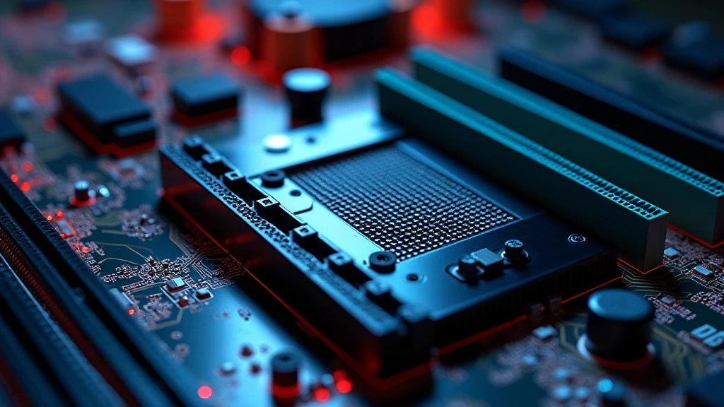
CMOS, Complementary Metal-Oxide-Semiconductor, is a small, low-power SRAM chip on every modern motherboard, kept alive by a CR2032 coin cell even when the system is fully powered off. It stores the Real Time Clock (RTC) registers, BIOS/UEFI configuration tables, boot device priorities, hardware voltage offsets, memory timings, and any stored BIOS passwords. When that data becomes corrupted, mismatched to new hardware, or locked behind a forgotten password, a CMOS clear is the definitive corrective action. Understanding how to clear CMOS correctly, without damaging hardware or losing recoverable data, is a foundational skill for any PC builder, system integrator, or overclocker working with modern platforms in 2026.
What Exactly Is CMOS and Why Does It Need Clearing?
The CMOS chip sits on the motherboard’s Super I/O controller or, on modern Intel and AMD platforms, is integrated into the Platform Controller Hub (PCH) or chipset logic. It is powered by a dedicated 3V CR2032 lithium coin cell rated for three to ten years of standby life depending on BIOS polling frequency and ambient temperature. The BIOS/UEFI firmware reads this chip at every POST (Power-On Self-Test) cycle to reconstruct the system’s hardware configuration state. Before finalizing equipment decisions, refer to our comprehensive mix nvme and sata ssd comparison.
Data Stored in CMOS
- RTC registers: System date and time, maintained independently of the OS.
- BIOS/UEFI setup parameters: CPU base clock, multiplier overrides, core voltage offsets, power limits (PL1/PL2/PPT/TDC/EDC).
- Memory configuration: XMP 3.0 or AMD EXPO profile selection, primary and secondary timing tables, DRAM voltage.
- Boot device order: NVMe, SATA, USB, PXE network boot priority sequence.
- Security data: Supervisor password, user password, Secure Boot keys (if not stored in dedicated SPI flash).
- PCIe lane configuration: Bifurcation settings, ASPM states, link speed overrides relevant to the PCI-SIG PCIe Specification Standard.
Common Triggers Requiring a CMOS Clear
- System fails POST after an aggressive or unstable overclock, CPU or memory settings rendered the platform unbootable.
- Forgotten BIOS supervisor password blocking access to firmware settings.
- New CPU installed that is incompatible with the current saved voltage/frequency tables.
- BIOS update corrupted the stored configuration profile.
- No video output despite known-good GPU and display, BIOS is looping on a bad boot device or corrupt handshake state.
- System clock drifting dramatically, indicating a dying coin cell that is also corrupting adjacent CMOS registers.
Method 1, BIOS/UEFI Software Reset (Preferred When System Boots)
If the system POSTs and reaches the BIOS/UEFI interface, the software reset path is the cleanest option because it writes verified factory-default values without requiring physical motherboard access. This method is suitable for any platform, consumer AM5, LGA1851, LGA1700, or server-grade boards, and is the recommended first step in any how to clear CMOS guide workflow.
Step-by-Step Procedure
- Power on the system and press the BIOS entry key immediately, typically Delete, F2, or F10 depending on the board vendor.
- Navigate to the Exit tab or equivalent menu (ASUS calls it “Exit,” MSI labels it “Save & Exit,” Gigabyte uses “Save & Exit Setup”).
- Select Load Optimized Defaults, Reset to Default, or Load Setup Defaults, the exact label varies by vendor and BIOS version.
- Confirm the action when prompted. The BIOS writes default values to CMOS and restarts.
- Re-enter BIOS after reboot, set the correct date/time, re-enable XMP/EXPO if desired, and configure boot order.
This method does not discharge the coin cell and does not affect the RTC hardware oscillator. It is the lowest-risk path and covers the majority of common scenarios including post-overclock recovery on high-end boards like those compared in the ASUS ROG Maximus Z890 Hero vs MSI MEG Z890 ACE feature analysis.
Method 2, CLR_CMOS Jumper (Universal Hardware Method)
Every ATX, Micro-ATX, and Mini-ITX motherboard produced in the last two decades includes a CLR_CMOS or JBAT1 three-pin (or two-pin) header on the PCB. This is the definitive hardware-level reset when the system cannot POST, when video output is absent, or when the BIOS is completely inaccessible. The jumper physically shorts two pads that drain the CMOS voltage rail through a bleed resistor network, forcing the SRAM to lose its stored state. For broader ecosystem context, read through our operational guide on pcie riser cable signal degradation.
Locating the Jumper
- Consult the motherboard manual, the jumper location is shown on the component layout diagram, usually labeled CLR_CMOS, JBAT1, CLRTC, or CMOS_SW.
- Physical location varies: near the coin cell holder on most consumer boards, near the rear I/O panel on some ITX designs, or along the bottom PCB edge on E-ATX server boards.
- The header is typically color-coded yellow or white and sits adjacent to a printed silkscreen label.
Step-by-Step Jumper Procedure
- Full power-down: Shut down the OS, power off the PSU via the rear rocker switch, then press the power button once to discharge the 5VSB rail from the capacitor bank. This is mandatory, clearing CMOS with 5VSB present can cause incomplete resets on some boards.
- Ground yourself: Touch a bare metal chassis surface or use an anti-static wrist strap before handling the PCB.
- Move the jumper: On a three-pin header, the jumper cap normally bridges pins 1 to 2 (normal operation). Move it to bridge pins 2 to 3 (clear position). On a two-pin header, place the jumper cap across both pins.
- Wait 15 to 30 seconds: This allows the bleed resistors to fully drain the CMOS SRAM capacitance. Some engineers recommend 60 seconds on older or high-leakage boards.
- Return jumper to normal position: Move the cap back to pins 1 to 2. Failure to do so means the board will re-clear CMOS on every boot.
- Reconnect power and boot: The system will POST with default settings. Expect a date/time error prompt, this is normal and expected.
Platforms built for aggressive overclocking, such as the processors reviewed in the AMD Ryzen 5 9600X vs Intel Core Ultra 5 245K comparison, frequently require the jumper method after a failed all-core frequency or fabric clock push that prevents POST.
Method 3, Dedicated CLR_CMOS Button
Premium and enthusiast-class motherboards, ASUS ROG Apex, MSI MEG, Gigabyte Aorus Master, ASRock Taichi, integrate a physical push-button labeled CLR_CMOS or RESET CMOS either on the PCB itself or accessible through the rear I/O shield cutout. This button performs the identical electrical function as the jumper method but eliminates the need to open the case or handle a jumper cap, making it the fastest hardware reset path for a system installed in a closed chassis.
Button Usage Procedure
- Power down the system completely and switch off the PSU rear rocker.
- Discharge the 5VSB rail by pressing the front-panel power button once.
- Press and hold the CLR_CMOS button for 10 to 15 seconds. Some boards require only a momentary press; the manual specifies which behavior applies.
- Release the button and restore PSU power.
- Boot normally, BIOS will load factory defaults.
Rear I/O mounted CLR_CMOS buttons are particularly useful in rack or test-bench environments where the board is powered but a POST failure has occurred and physical PCB access is restricted. Boards with rear I/O buttons are a key differentiator worth considering when reviewing desktop CPU benchmarks & reviews platforms for overclocking rigs.
Method 4, Physical Battery Removal
Battery removal is the fallback method for boards lacking a CLR_CMOS jumper or button (rare, but found on some OEM/prebuilt boards and early Mini-ITX designs) or when the jumper method fails to fully drain the CMOS, which can occur if a solder-bridged jumper header is present but the bleed circuit is open due to PCB damage.
Battery Removal Procedure
- Complete full shutdown and PSU power-off as described in Method 2.
- Discharge 5VSB rail via front-panel power button press.
- Locate the CR2032 coin cell, typically in a horizontal or vertical retention clip near the PCIe x16 slot.
- Use a non-conductive plastic spudger or fingernail to depress the retention clip and slide the battery out. Do not use metal tools near the PCB to avoid shorting adjacent components.
- Wait a minimum of 5 minutes, ideally 15 to 30 minutes. Modern PCBs include bulk capacitance on the CMOS power rail that can sustain the SRAM state for several minutes after battery removal. A shorter wait risks incomplete erasure.
- Reinsert the battery, restore PSU power, and boot. If the coin cell voltage tests below 2.8V on a multimeter, replace it with a fresh Panasonic or Energizer CR2032, do not reinstall a depleted cell.
A dying coin cell below 2.5V not only fails to maintain CMOS state but can corrupt RTC registers in ways that cause intermittent POST failures, incorrect system clock, or even PCIe enumeration errors that affect GPU detection, a problem worth cross-referencing with graphics card tests & GPU guides when diagnosing no-display scenarios.
CMOS Clear Method Comparison Table
| Method | System Must Boot? | Case Open Required? | Time Required | Risk Level | Best Use Case |
|---|---|---|---|---|---|
| BIOS Software Reset | Yes, BIOS must be accessible | No | <2 minutes | Very Low | Clearing bad OC profile, refreshing defaults |
| CLR_CMOS Jumper | No | Yes | 2 to 5 minutes | Low (ESD risk only) | No-POST scenarios, locked BIOS password |
| CLR_CMOS Button | No | No (rear I/O) or Yes (PCB button) | 1 to 2 minutes | Very Low | Enthusiast boards, closed-chassis recovery |
| Battery Removal | No | Yes | 15 to 30 minutes | Low-Medium | No jumper present, OEM/prebuilt boards |
| Shorting Battery Contacts | No | Yes | 30 to 60 seconds | Medium (PCB risk if misapplied) | Last resort, soldered battery, expert only |
Post-Reset Configuration: What to Restore After Clearing CMOS
A CMOS clear returns every BIOS parameter to factory defaults, which is intentional but requires deliberate reconfiguration before the system is production-ready. Skipping this step results in degraded memory performance (DRAM running at JEDEC 4800 MT/s instead of its XMP 6400 MT/s profile, for example), incorrect power limits that throttle CPU performance, and potentially incorrect Secure Boot key state.
Mandatory Post-Reset Steps
- Set system date and time, CMOS clear wipes the RTC registers. Set these before any OS boot to prevent log corruption and certificate validation errors.
- Enable XMP 3.0 or AMD EXPO, DRAM defaults to the lowest JEDEC-compliant frequency and relaxed timings after a reset. Re-enable the manufacturer’s validated XMP/EXPO profile for rated performance. This is particularly impactful on platforms evaluated in Radeon RX 9060 XT 8GB vs 16GB comparison testing where memory bandwidth directly affects GPU frame pacing.
- Reconfigure boot order, Restore the primary NVMe or SATA boot drive to the top of the boot priority list.
- Re-enable Secure Boot, If required by the OS (Windows 11 mandates Secure Boot for full TPM 2.0 compliance), navigate to the Security tab and restore Secure Boot state.
- Restore CPU power limits, Boards from ASUS, MSI, and Gigabyte often default to unrestricted or “Auto” power limits post-reset, which may differ from the manually configured PL1/PL2 values previously set. Verify these match your thermal solution’s capacity.
- Reconfigure fan curves, All Q-Fan, Smart Fan, or custom PWM profiles are erased. Default curves are conservative but may result in higher acoustic output than a tuned profile.
- Re-enter BIOS password, If a supervisor password is required for security compliance, re-establish it after confirming all other settings are correct.
Final Diagnostic Verdict & Maintenance Checklist
A CMOS clear is not a fix for underlying hardware failure, it resolves configuration-state problems exclusively. If the system still fails to POST after a successful CMOS clear confirmed by the jumper method with the 30-second wait, the fault is hardware: failed CPU, seated-improperly or incompatible DRAM, dead PSU rail, or a shorted motherboard trace. The CMOS clear eliminates software/firmware state as a variable, which is precisely its diagnostic value in pc hardware 2026 troubleshooting workflows.
Pre-Clear Checklist
- Document all current BIOS settings (photograph the BIOS screens or use the BIOS profile export function if available) before clearing, some data is unrecoverable.
- Confirm PSU rear switch is off and 5VSB rail is discharged before any physical method.
- Use ESD precautions on bare PCB work, especially when handling HEDT or server-class boards with dense component populations.
- Identify the correct jumper header from the motherboard manual before moving any cap, misidentifying the header can short adjacent diagnostic or debug pins.
Post-Clear Verification Checklist
- System POSTs cleanly and reaches BIOS without looping, confirms CMOS state is valid.
- DRAM is detected at correct capacity and speed under JEDEC default (XMP not yet applied).
- All storage devices are enumerated in the boot device list.
- Date and time are set correctly before first OS boot.
- XMP/EXPO re-enabled and validated with a brief memtest pass (minimum 1 cycle of MemTest86 or Windows Memory Diagnostic).
- CPU temperatures under load are within expected range, default power limit changes post-reset can affect thermal envelope.
- Coin cell voltage measured at or above 2.8V, replace if below threshold to prevent repeat CMOS corruption within months.
Clearing CMOS is one of the most reliable first-response tools in hardware diagnostics. Executed correctly, with full power removal, appropriate wait times, and systematic post-reset reconfiguration, it resolves the majority of firmware-state failures in minutes and provides a clean baseline from which to rebuild a stable, validated platform configuration.
Notes on Resetting Board Settings
Clearing CMOS usually means cutting power and either moving a jumper or removing the coin cell for a short time. Owners wanting a broader look at board layouts can continue with motherboards, which covers similar hardware.
Readers wanting general electrical safety background for equipment work can look at American National Standards Institute (ANSI) as a neutral reference.