
Quick Answer
XMP (Intel), EXPO (AMD), and DOCP (ASUS) are one-click BIOS profiles that push RAM beyond JEDEC baseline frequencies. XMP targets Intel platforms; EXPO targets AMD AM5/AM4; DOCP is ASUS’s XMP relay for AMD boards. All three are safe, vendor-certified overclocks, choose the profile matching your CPU platform.

Pros
- Fast 6000MHz DDR5 specification suits performance-focused desktop builds.
- Works with both AMD EXPO and Intel XMP 3.0 platforms.
- 32GB capacity is a practical sweet spot for gaming and multitasking.
- Broad motherboard support across AMD 600/800 series and Intel 600/700/800 series boards.
Cons
- Premium pricing may put it above many standard 32GB DDR5 kits.
- Rated performance depends on a compatible motherboard and enabling EXPO or XMP in BIOS.
- CL36 is solid, but not the lowest latency available in high-end DDR5 memory.
Overview: The Corsair Vengeance DDR5 32GB kit is a desktop memory upgrade built for users who want fast, modern DDR5 performance in a clean gray design. It uses a 2x16GB dual-channel layout, which is a practical fit for gaming systems, creator PCs, and performance desktops.
Performance and features: With a 6000MHz rated speed and CL36-44-44-96 timings, this kit is aimed at strong everyday responsiveness and improved throughput in demanding tasks. AMD EXPO and Intel XMP 3.0 support make it easier to load optimized memory profiles, while onboard voltage regulation adds more control for users who want to tune performance further.
Drawbacks and considerations: This is a premium memory kit, so buyers should expect to pay more than with basic DDR5 options. Also, getting the advertised speed typically depends on a compatible motherboard and enabling the correct memory profile in BIOS, and CL36 is good but not class-leading for latency.
Verdict: The strongest value comes from users building or upgrading a high-performance AMD or Intel desktop who want fast DDR5, broad compatibility, and simpler overclocking support. It is less compelling for budget-focused buyers who only need standard memory speeds.

Pros
- Fast DDR5 6000MHz CL30 specification is well suited to gaming and high-performance desktop use.
- Low 34 mm profile helps with RAM and CPU cooler clearance.
- Supports both Intel XMP 3.0 and AMD EXPO for easier setup on compatible systems.
- Premium aluminum heatsink and white finish suit clean, modern PC builds.
Cons
- Requires a DDR5-compatible motherboard and platform, so it is not usable in DDR4 systems.
- Full advertised performance depends on motherboard and CPU support for XMP or EXPO profiles.
- The listing does not provide a complete set of secondary timings or warranty details, which may matter for comparison shopping.
Overview: The KLEVV Bolt V DDR5 32GB (2x16GB) 6000MHz CL30 kit is a white desktop memory set built for modern gaming and high-performance PCs. Its minimalist aluminum heatsink and 34 mm low-profile design make it easy to fit in many builds.
Performance: With DDR5 6000MT/s speed, CL30 latency, SK Hynix A-Die ICs, and 1.35V operation, this kit is aimed at responsive gaming, multitasking, and creator workloads. Intel XMP 3.0 and AMD EXPO Ready profiles help simplify setup on supported platforms.
Drawbacks: It is a DDR5-only upgrade, so older DDR4 systems cannot use it. Also, achieving the advertised tuning depends on motherboard and CPU support, and the listing does not provide a full set of secondary timings or warranty details.
Verdict: Choose this kit if you want a compact, premium-looking 32GB DDR5 memory upgrade for a gaming or enthusiast build and your platform supports XMP or EXPO. It is best suited to users who value speed, clearance, and a clean white aesthetic.

Pros
- Rated speed of 6000MHz with CL36-38-38-80 extended timings
- Supports both Intel XMP 3.0 and AMD EXPO overclocking profiles
- Includes two 16GB modules for 32GB dual-channel desktop memory
- Tested at component and module levels by Micron
Cons
- Requires compatible DDR5-capable processors and motherboards
- Minimalist design offers no RGB illumination options
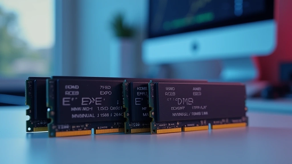
Every DDR5 kit sold today ships clocked at a conservative 4800 MT/s JEDEC baseline, yet the sticker on the box reads 6000, 6400, or even 8000 MT/s. That gap exists because DRAM manufacturers program secondary timing and voltage data into the module’s SPD (Serial Presence Detect) chip as named profiles, which the BIOS reads and applies in a single toggle. Intel’s ecosystem calls this mechanism XMP (Extreme Memory Profile); AMD’s native implementation is EXPO (Extended Profiles for Overclocking); and ASUS bridges the gap on AMD motherboards with DOCP (Direct Overclock Profile). Understanding the xmp vs expo difference is not optional for any builder targeting peak system throughput in 2026, it is the lowest-cost, highest-return tuning step available before touching any manual timing slider.
The SPD Architecture Behind All Three Standards
What the Serial Presence Detect Chip Actually Stores
Every DDR4 and DDR5 DIMM carries a small EEPROM, the SPD chip, soldered directly to the module PCB. The JEDEC Memory Standards Specification defines Bytes 0 to 127 of this EEPROM for baseline interoperability data: default frequency, primary timings (CL, tRCD, tRP, tRAS), and supply voltage. Everything beyond that baseline is vendor territory. XMP uses a defined extension block in the upper SPD bytes to store up to three discrete profiles, each containing a complete set of frequency, sub-timings, voltage targets, and training hints. The BIOS reads whichever profile the user selects and programs the memory controller accordingly, no manual entry required.
DDR5 SPD Hub: The Hardware Change That Matters
DDR5 introduced a critical architectural shift: the SPD is no longer a passive EEPROM but an active SPD Hub (SPD5118 controller) with an I3C interface. This hub manages write-protect logic, so the BIOS can read but not corrupt profile data accidentally. It also enables newer features like on-die ECC reporting and temperature sensor integration through a unified bus. When you enable XMP or EXPO on a DDR5 system, the SPD hub confirms the profile handshake with the IMC (Integrated Memory Controller) before training begins , a more robust sequence than DDR4’s passive read model. To compare alternative configurations, check our hands-on review of set pagefile size windows 11.
Intel XMP: Specification Deep Dive
XMP 1.0, 2.0, and 3.0, What Changed Each Generation
Intel introduced XMP 1.0 alongside DDR3 in 2007. XMP 2.0 arrived with DDR4, expanding profile count to two and adding tighter timing granularity. XMP 3.0, released with DDR5 and Intel’s Alder Lake (12th Gen) platform, is the current standard and the version builders in 2026 will encounter on virtually all retail kits. XMP 3.0 supports up to five profiles: two user-writable slots (allowing end-user customization saved back to SPD), two vendor-defined fixed profiles, and one base JEDEC profile. It also adds an Optimized Profile flag that lets the module communicate recommended training parameters to the IMC for improved boot reliability at high frequencies.
XMP Voltage and Frequency Ranges for DDR5
Standard DDR5 JEDEC baseline runs at 1.10 V. XMP 3.0 profiles for aggressive DDR5 kits target 1.35 V to 1.45 V at frequencies between 6000 and 8400 MT/s. Intel’s IMC on Raptor Lake Refresh (13th/14th Gen) and Meteor Lake officially supports up to DDR5-5600 natively, but validated XMP profiles extend that envelope through controlled IMC training. Arrow Lake (Core Ultra 200S) raised native DDR5 support ceilings, making 6400 MT/s XMP profiles boot reliably on first attempt. For builders evaluating platform choices around memory bandwidth, the AMD Ryzen 5 9600X vs Intel Core Ultra 5 245K comparison breaks down real-world IMC behavior across both architectures.
AMD EXPO: Why AMD Built Its Own Standard
The Business and Technical Case for a Separate Ecosystem Profile
XMP is an Intel-owned, Intel-licensed specification. AMD has no obligation to validate XMP profiles against its own IMC behavior on AM4 or AM5 , and because Zen 4’s DDR5 IMC has a fundamentally different training algorithm, voltage sequencing, and command-rate sensitivity compared to Intel’s IMC, applying an XMP profile on a Ryzen system produces inconsistent results: occasional boot failures, elevated training errors, or frequency shortfalls. AMD launched EXPO in late 2022 alongside the Ryzen 7000 AM5 platform to solve this: EXPO profiles are certified on AMD’s own IMC, using AMD-validated voltage curves and sub-timings. An EXPO-certified kit at DDR5-6000 is guaranteed to boot correctly on a Zen 4 board that lists that kit as validated , XMP at the same frequency carries no such guarantee. Users looking for related component recommendations can explore our check ram die type breakdown.
EXPO Profile Structure and Dual-Profile Support
EXPO stores two profiles in the SPD extension block. Profile 1 is typically the headline frequency with tightened primary timings (for example, DDR5-6000 CL30). Profile 2 is a relaxed-timing alternative at the same or slightly lower frequency, designed for maximum boot compatibility on boards with conservative training defaults. Both profiles include full secondary and tertiary timing sets, VDDQ targets, VDD targets, and IMC training hints specific to AMD’s memory controller. The EXPO block coexists with XMP data on dual-certified kits, a single DIMM can carry both an EXPO block and an XMP 3.0 block, letting the board choose the correct profile automatically based on platform detection.
EXPO and the AM5 Sweet Spot: DDR5-6000
Zen 4’s memory subsystem performs optimally when MCLK (memory clock), UCLK (Unified Memory Controller clock), and FCLK (Infinity Fabric clock) run in a 1:1:1 ratio. That ratio locks at DDR5-6000 on most Ryzen 7000 and Ryzen 9000 boards without requiring manual UCLK decoupling. DDR5-6000 EXPO kits are therefore the single highest-value memory upgrade for AM5 systems, beyond 6000 MT/s the memory subsystem decouples, adding latency that partially cancels the bandwidth gain. Motherboard platforms like those reviewed in the ASUS ROG Maximus Z890 Hero vs MSI MEG Z890 ACE comparison demonstrate how flagship board designs implement EXPO training differently, affecting cold-boot reliability at DDR5-6000 and above.
ASUS DOCP: The Translation Layer Explained
Why DOCP Exists on ASUS AMD Motherboards
Before EXPO existed, AMD system builders who wanted to run DDR4 or early DDR5 above JEDEC speeds faced a problem: XMP profiles were present on the stick, but AMD motherboard BIOSes lacked an “Enable XMP” toggle because XMP is Intel-branded. ASUS introduced DOCP as a relabeled XMP reader , the BIOS reads the XMP SPD block and applies those timings, voltages, and frequencies identically, but presents the option under an AMD-neutral name. Functionally, DOCP Profile 1 = XMP Profile 1. There is no technical difference in what gets programmed to the memory controller; only the UI label changes. Before finalizing equipment decisions, refer to our comprehensive sodimm in desktop pc comparison.
DOCP in 2026: Largely Superseded but Still Present
On modern AM5 boards running EXPO-certified DDR5, DOCP is rarely the correct choice, use the native EXPO profile instead. DOCP remains relevant for two scenarios: legacy AM4 DDR4 systems where EXPO does not exist, and DDR5 kits that carry XMP 3.0 profiles but no EXPO block (typically Intel-targeted kits installed in an AMD system). Other motherboard vendors have equivalent implementations: MSI calls theirs A-XMP, Gigabyte uses EOCP, and ASRock labels it AMP. All relay the XMP SPD block without modification.
Head-to-Head Specification Comparison
| Attribute | Intel XMP 3.0 | AMD EXPO | ASUS DOCP |
|---|---|---|---|
| Standard Owner | Intel Corporation | AMD Inc. | ASUS (XMP relay) |
| Target Platform | Intel LGA 1700, LGA 1851 | AMD AM5, AM4 (DDR4) | AMD AM4, AM5 (ASUS boards) |
| DRAM Generation | DDR3, DDR4, DDR5 | DDR4, DDR5 | DDR4, DDR5 |
| Max Profiles Stored | 5 (3.0); 2 (2.0) | 2 | 2 (mirrors XMP slots) |
| User-Writable Profiles | Yes (XMP 3.0 slots 4 to 5) | No | No |
| IMC Validation Source | Intel IMC labs | AMD IMC labs | Intel IMC labs (via XMP) |
| Typical DDR5 Voltage | 1.25 V – 1.45 V | 1.25 V – 1.40 V | 1.25 V – 1.45 V |
| Common DDR5 Frequencies | 5600 to 8400 MT/s | 5600 to 8000 MT/s | 5600 to 8400 MT/s |
| Dual-Certified Kits | Yes (XMP + EXPO on same DIMM) | Yes | N/A (reads whichever block exists) |
| Warranty Impact | None (DRAM vendor supports) | None (DRAM vendor supports) | None (DRAM vendor supports) |
| CPU Warranty Impact | Technically voids Intel’s OC warranty clause; rarely enforced | No impact; AMD explicitly supports EXPO | Same as XMP on AMD |
Performance Impact, Compatibility Pitfalls, and Platform Guidance
Real-World Bandwidth and Latency Deltas
Running DDR5 at JEDEC 4800 MT/s versus an EXPO/XMP 6000 MT/s profile delivers measurable gains across bandwidth-sensitive workloads. Game scene streaming, texture decompression, and physics simulation in titles using DX12 async compute show 5 to 12% frame-time improvement at the same GPU load, a free gain from a BIOS toggle. Content creation applications such as Blender’s CPU path tracer and HandBrake’s x265 encoder show 3 to 8% throughput improvements. The gains compound when paired with a fast GPU: for context on how memory bandwidth interacts with GPU performance tiers, the Radeon RX 9060 XT 8GB vs 16GB comparison demonstrates vRAM bandwidth bottlenecks that a faster system memory bus can partially alleviate in CPU-limited scenarios.
Common Failure Modes and Diagnostic Symptoms
Enabling an XMP profile on an AMD board without an EXPO block, or applying EXPO on an Intel board, does not destroy hardware. The most likely outcomes are: POST failure (three DRAM debug LEDs), automatic BIOS rollback to JEDEC defaults, Windows BSOD with WHEA_UNCORRECTABLE_ERROR, or intermittent memory training failure on cold boots. Dual-rank configurations at high frequency are the most common instability source; dropping from XMP Profile 1 to Profile 2, or reducing frequency by one step (e.g., 6400 u2192 6000 MT/s), resolves the majority of cases without manual timing adjustment. Builders researching platform-level IMC robustness for desktop CPU benchmarks & reviews will find IMC stress scores correlated with DRAM training reliability across frequency tiers.
Which Profile to Enable on Each Platform
- Intel LGA 1700 / LGA 1851 (12th-15th Gen, Core Ultra 200S): Enable XMP 3.0 Profile 1. If the kit is dual-certified, the board auto-selects XMP. Manual override: BIOS u2192 AI Tweaker / Memory u2192 XMP u2192 Profile 1.
- AMD AM5 (Ryzen 7000 / 9000): Enable EXPO Profile 1 on EXPO-certified kits. On non-EXPO kits, use DOCP/A-XMP/EOCP. Prioritize DDR5-6000 for 1:1:1 clock ratio.
- AMD AM4 (Ryzen 3000 / 5000, DDR4): Use DOCP (ASUS), A-XMP (MSI), or EOCP (Gigabyte). EXPO does not exist for DDR4; all profiles relay XMP data.
- Mixed or uncertain platform: Enable whichever profile the board presents as the primary option, modern BIOSes on 2025 to 2026 boards detect platform and surface the correct standard automatically.
Adoption Rate and Kit Availability in 2026
As of 2026, EXPO adoption has reached near-parity with XMP on mainstream DDR5 kits priced above $60 per kit. Corsair, G.Skill, Kingston, Crucial, and TeamGroup all ship dual-certified (XMP 3.0 + EXPO) kits across their performance DDR5 lines. Budget DDR5 kits at the entry tier ($40 to 55) often carry XMP-only profiles, a meaningful consideration for AMD builders who should specifically search product listings for “EXPO” certification before purchasing. For a comprehensive view of how platform choices drive memory specification decisions in 2026 system builds, the graphics card tests & GPU guides section contextualizes total platform bandwidth budgeting across CPU, RAM, and GPU tiers.
Final Diagnostic Verdict & Maintenance Checklist
The xmp vs expo difference reduces to a single engineering principle: each standard was validated against a specific IMC architecture. XMP on Intel, EXPO on AMD, using the wrong profile is not dangerous, but it introduces unnecessary training risk that the correct profile eliminates entirely. DOCP is not a third standard; it is a UI alias for XMP on AMD boards and carries all XMP characteristics, including the lack of AMD IMC validation.
For pc hardware 2026 builds, dual-certified DDR5 kits are the universal answer, they coexist on one DIMM, cost identically to single-certified kits at the same bin, and eliminate the compatibility decision entirely. The only remaining step is enabling the correct profile in BIOS, which takes under 60 seconds.
Pre-Boot Configuration Checklist
- Confirm kit certification: check the manufacturer’s QVL (Qualified Vendor List) for your specific motherboard model.
- Update BIOS to the latest stable release, memory training algorithms improve significantly across BIOS revisions, particularly on AM5.
- Install DIMMs in the correct slots, typically A2/B2 (slots 2 and 4) for dual-channel; incorrect slot population disables XMP/EXPO at high frequencies on many boards.
- Enter BIOS u2192 navigate to memory/AI Tweaker section u2192 enable XMP (Intel), EXPO (AMD), or DOCP/A-XMP/EOCP (AMD non-EXPO kits).
- Select Profile 1 as the first attempt; revert to Profile 2 if POST fails three consecutive times.
- Verify applied settings post-boot using CPU-Z (Memory tab), confirm frequency matches the profile target and timings match the SPD-stored values.
- Run 30-minute memory stability validation using TestMem5 with the anta777 Extreme preset before considering the system stable.
- If instability persists at Profile 1 on AM5: manually set VDDQ to 1.35 V (for 6000 MT/s kits) and enable RTTPARK termination optimization in BIOS, resolves the majority of Zen 4 DDR5 training failures without reducing frequency.
- For Intel platforms at DDR5-7200+: enable Gear 2 mode if training failures persist; Gear 2 halves UCLK relative to MCLK, trading latency for stability headroom at extreme frequencies.
- Document working BIOS settings and export a BIOS profile backup before any firmware update, training parameters occasionally reset to JEDEC defaults after major BIOS revisions.
Reading on Memory Profiles
XMP, DOCP, and EXPO are vendor profile formats that store faster memory settings for the firmware to load. Background on electronics terms, such as the material at American National Standards Institute (ANSI), can make board manuals easier to read.