
Quick Answer
AM5 DDR5 slow boot is caused by per-boot memory training, a full impedance, voltage, and timing calibration the CPU must run each POST cycle. Enabling Memory Context Restore in UEFI caches those trained parameters in SPI flash, cutting cold-boot POST from 60 to 90 seconds to under 20 seconds with no stability penalty when EXPO timings are stable.

Pros
- Rated for speeds up to 6400MT/s with AMD EXPO profile
- Tight CL30-39-39-102 latency timings at 1.40V
- Designed and validated for AMD X870, X670, and B650 platforms
Cons
- Requires manual BIOS overclocking to exceed base JEDEC speeds
- Peak speed depends heavily on motherboard and CPU capability

Pros
- 32GB capacity handles demanding games, multitasking, and creative workloads
- 6000MT/s speed with CL30 latency is well suited for AMD Ryzen performance
- AMD EXPO profiles make enabling rated speeds simple in BIOS
- FURY Beast series is a well known Kingston memory line for desktop builds
Cons
- DDR5 memory requires a DDR5 compatible motherboard, so it will not work with older DDR4 systems
- EXPO is designed for AMD platforms, so Intel users may need to rely on XMP or manual settings
The Kingston FURY Beast 32GB 6000MT/s DDR5 CL30 is best for AMD builders who want high capacity memory with easy overclocking through EXPO profiles. The 6000MT/s speed and CL30 latency pair well with modern Ryzen systems for responsive gaming and multitasking. The main trade-off is that this is DDR5 only, so it requires a compatible DDR5 motherboard and will not fit older DDR4 systems.
Capacity: 32GB
Type: DDR5
Speed: 6000MT/s
Latency: CL30
Overclocking: AMD EXPO
Pros
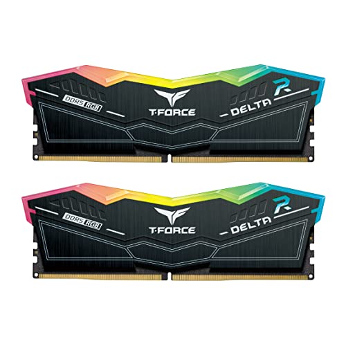
- Very high 7200MHz DDR5 speed rating for a performance-focused desktop build.
- 32GB capacity in a 2x16GB configuration supports dual-channel operation.
- XMP 3.0 support makes performance tuning more convenient on compatible boards.
- Power management ICs are included for stable and efficient power usage.
Cons
- Requires a compatible 600 or 700 series chipset platform to fully benefit from its rated performance.
- High-speed DDR5 kits like this can be more expensive than lower-frequency alternatives.
- RGB lighting may add value for some users but is unnecessary for buyers focused only on raw performance.
Overview & Design: The TEAMGROUP T-Force Delta RGB DDR5 32GB kit is a desktop memory upgrade built around a 2x16GB layout, 7200MHz speed, and CL34 timings. It is designed for users who want a performance-oriented RAM kit with an RGB look for modern gaming or creator PCs.
Performance & Key Features: Its high frequency, XMP 3.0 readiness, and A-DIE design make it a strong fit for demanding workloads where memory bandwidth matters. The included power management ICs are intended to support stable and efficient power usage, and the kit is aimed at 600 and 700 series chipset systems that can take advantage of fast DDR5 memory.
Drawbacks & Considerations: This is a premium-spec kit, so it is best suited to users with a compatible motherboard and CPU platform. Buyers should also remember that very fast DDR5 can depend heavily on system compatibility, and RGB lighting adds visual appeal rather than direct performance.
Verdict: The T-Force Delta RGB DDR5 32GB 7200MHz CL34 kit makes the most sense for enthusiasts, gamers, and creators building a compatible high-performance desktop. If you want fast DDR5 memory with a polished design and easy profile support, it is a strong option to consider.

Pros
- Fast 6000MHz rated speed with tight CL30-36-36-76 timings
- Ten individually addressable RGB LEDs per module
- Supports AMD EXPO and Intel XMP profiles
- Onboard voltage regulation manageable via CORSAIR iCUE
Cons
- Advertised 6000MHz speed requires manual BIOS overclocking
- Higher 1.77-inch profile may affect compact cooler clearances

Pros
- High 6000MT/s rated speed for a performance-focused DDR5 kit.
- Low CL30 timing is attractive for gamers and PC enthusiasts.
- Works with both Intel XMP 3.0 and AMD EXPO platforms.
- Includes an aluminum heatsink for improved thermal management.
- Backed by a lifetime warranty for long-term ownership confidence.
Cons
- Advertised speeds require compatible motherboard, CPU, and BIOS profile support.
- This is unbuffered UDIMM desktop memory, so it is not intended for laptops or server systems.
- Full performance depends on system configuration, so plug-and-play speeds may run at JEDEC defaults until profiles are enabled.
Overview & Design: The SP Silicon Power Value Gaming DDR5 32GB kit is a desktop memory upgrade made for users who want fast DDR5 performance in a standard 2x16GB UDIMM layout. The aluminum heatsink gives it a practical, heat-conscious design that fits a performance PC build.
Performance & Key Features: Rated at 6000MT/s with CL30 timings and 1.35V operation, this kit is aimed at responsive gaming and demanding multitasking. Support for Intel XMP 3.0 and AMD EXPO makes it easier to run the advertised profile on compatible systems, while the integrated PMIC helps support more stable power delivery.
- 32GB total capacity in a dual-channel 2x16GB kit
- 6000MT/s rated speed with CL30 timing
- XMP 3.0 and AMD EXPO support
- Aluminum heatsink for thermal management
- Lifetime warranty coverage
Drawbacks & Considerations: The main limitation is compatibility, since the advertised speed depends on the motherboard, CPU, and BIOS profile support. As with most high-speed DDR5 kits, plug-and-play behavior may default to JEDEC standards until XMP or EXPO is enabled.
Verdict: This kit makes the most sense for desktop gamers and PC builders who want a fast 32GB DDR5 upgrade with easy profile-based tuning. If your platform supports 6000MT/s DDR5 and you want a balanced mix of speed, cooling, and warranty coverage, it is a strong option to consider.
What Memory Training Actually Does at the Silicon Level
DDR5 eliminated the on-DIMM voltage regulator from DDR4 and moved power delivery onto the module itself via an integrated PMIC (Power Management IC). Simultaneously, the memory controller migrated fully onto the CPU die , on AM5, that is AMD’s Unified Memory Controller embedded within the Zen 4 and Zen 5 I/O die. This architecture delivers higher bandwidth and tighter voltage control, but it demands that the memory controller and each DRAM die negotiate a fresh electrical handshake at every power cycle unless explicitly told otherwise. For broader ecosystem context, read through our operational guide on set pagefile size windows 11.
The Four Phases of DDR5 Training
During POST, the AMD AGESA (AMD Generic Encapsulated Software Architecture) firmware executes memory training in four distinct phases that run sequentially and cannot be parallelized:
- ZQ Calibration: The memory controller measures the physical impedance of the transmission lines between the CPU’s DDR5 PHY and each DRAM die. Ambient temperature, PCB trace length, and DIMM slot population all shift these values. ZQ runs first because every subsequent phase depends on accurate impedance matching to prevent signal reflection at high data rates.
- Write Leveling: DDR5 uses a fly-by topology where the clock signal arrives at each DRAM chip at slightly different times due to trace length differences. Write leveling adjusts the DQS (Data Strobe) delay per byte lane so all write transactions are aligned to the clock edge at the receiving die, not at the source.
- Read/Write DQ Bit Deskew: Each of the 64 data bits (plus ECC bits on ECC-capable platforms) has individual propagation delay caused by PCB routing asymmetry. AGESA sweeps delay values per bit to find the maximum valid eye opening, the timing window where a ‘1’ or ‘0’ is read reliably. On EXPO kits at DDR5-6000 or above, this sweep is wider and more granular, taking measurably longer than at JEDEC-spec DDR5-4800.
- VREF Training: The internal reference voltage for both the CA (Command/Address) bus and the DQ (Data) bus is swept to find the center of the voltage margin window. DDR5 performs this digitally on-die via the Mode Register, unlike DDR4 where VREF was set externally.
The full four-phase sequence on a two-DIMM AM5 system at DDR5-6000 EXPO takes 45 to 90 seconds at cold ambient temperatures. At elevated temperatures (above 35°C case ambient) AGESA sometimes detects marginal signal integrity and repeats training passes, extending POST further. The JEDEC Memory Standards Specification mandates that compliant DDR5 controllers perform fresh training after any power-down event where DRAM content is lost, which is every normal shutdown or power loss.
Why EXPO Makes Training Slower Than XMP
Intel’s XMP 3.0 profiles target Intel memory controllers tuned to specific validated frequency and timing combinations. AMD’s EXPO profiles target Ryzen’s memory controller (UCLK/MEMCLK domain), which operates in a 1:1 (coupled) or 1:2 (decoupled) ratio mode. At DDR5-6000 on AM5, AGESA targets the 1:1 ratio, UCLK at 3000 MHz, which is the performance sweet spot but also the electrical limit of the silicon for most Zen 4/5 dies. Training at this boundary requires more sweeping passes, more retries on marginal signal eyes, and more VREF iterations. DDR5-6400 and above almost always forces 1:2 ratio, which trains faster but sacrifices memory controller latency. If you are building a high-performance AM5 system and evaluating CPU options, the AMD Ryzen 5 9600X vs Intel Core Ultra 5 245K comparison covers how these memory architecture differences translate into real-world application performance.
Memory Context Restore: What It Saves, What It Discards
Memory Context Restore (MCR) , called “Memory Fast Boot” on some older AGESA versions and exposed differently across vendors , works by serializing the trained register state from the previous successful boot into a reserved region of the motherboard’s SPI flash (the same chip that stores the UEFI firmware image). On the next cold boot, AGESA reads those cached parameters, programs them directly into the memory controller and DRAM mode registers, and skips the sweep phases entirely. For troubleshooting and reliability insights, consult our in-depth check ram die type report.
What Gets Cached
- ZQ calibration codes per byte lane
- Write leveling delay values per DIMM, per rank
- DQ read and write delay tap settings per bit
- CA and DQ VREF codes
- ODT (On-Die Termination) resistance programming
- Trained tRFC, tRCD, tCL, tWR values as resolved by AGESA (not necessarily what you set in BIOS, AGESA sometimes tightens or loosens what you specify based on silicon response)
What MCR Does Not Cache and Why It Matters
MCR does not cache temperature-compensated adjustments. If the system was trained at 22°C and powers on at 35°C case ambient, the cached impedance values are off. Modern AGESA versions (1.2.0.x and later for Zen 4, 1.3.0.x for Zen 5) include a thermal validity check, if the delta between stored-training temperature and current temperature exceeds a threshold (typically u00b115°C), AGESA discards the cache and performs a full retrain. This is the correct behavior and not a bug; marginal EXPO kits near the edge of signal integrity at elevated temperatures would produce silent data corruption if stale cold-trained parameters were applied at high thermal loads.
MCR also does not survive CMOS clears, BIOS updates, or any change to memory-related UEFI settings. Any of those three events invalidates the stored context and forces a full retrain on the next two boots (one to train, one to validate the trained state before caching). Plan BIOS updates around this , the first boot after a microcode update that touches AGESA will always be slow regardless of MCR state. Readers comparing setup options can review our technical analysis on sodimm in desktop pc.
Symptom Diagnostic Matrix
| Symptom | Duration | DRAM LED State | Root Cause | Correct Action |
|---|---|---|---|---|
| Black screen, DRAM LED solid, then boots normally | 30 to 90 s | Solid amber/white | Normal full memory training (MCR disabled or cache invalidated) | Enable Memory Context Restore in UEFI |
| Black screen, DRAM LED flashes, system reboots 2 to 3u00d7 then boots | 90 to 180 s total | Flashing, then solid, then off | EXPO training failure, AGESA retrying with relaxed timings | Increase DRAM voltage to 1.40 V; loosen tRFC; verify DIMM seating |
| Black screen, no POST, DRAM LED stays solid indefinitely | >3 min, no recovery | Solid, unresponsive | Incompatible EXPO profile or defective DIMM/slot | CMOS clear; boot at JEDEC DDR5-4800; test single DIMM in A2 slot |
| Fast POST (<20 s) then Windows memory error / BSOD | N/A | Normal (off during OS boot) | Stale MCR cache applied at different thermal state | Disable MCR, boot once to retrain, re-enable MCR |
| Slow boot only on first morning power-on, fast after that | 45 to 75 s first boot | Solid during training | Thermal delta exceeding MCR validity threshold (cold room) | Expected behavior; raise SoC voltage by +0.025 V to improve cold-boot margin |
| Slow boot persists even with MCR enabled | 30 to 60 s | Solid then off | AGESA version bug or MCR not writing to flash (SPI write protection) | Update BIOS; verify BIOS Flashback protection is not locking SPI region |
UEFI Configuration: Enabling Memory Context Restore by Vendor
Each major AM5 motherboard vendor exposes MCR and related boot-acceleration settings under different menu paths. The functional result is identical, cached training bypass, but the naming is inconsistent enough to confuse experienced builders. If you are evaluating which AM5 motherboard to purchase before configuring these settings, the ASUS ROG Maximus Z890 Hero vs MSI MEG Z890 ACE comparison covers how each board’s UEFI implementation handles EXPO stability and training behavior in detail.
ASUS AM5 Boards (ROG, ProArt, TUF, Prime)
- Enter UEFI u2192 press F7 for Advanced Mode.
- Navigate to Ai Tweaker u2192 DRAM Timing Control u2192 Memory Context Restore.
- Set to Enabled.
- Separately, navigate to Boot u2192 Boot Configuration u2192 Fast Boot and set to Enabled (this skips USB enumeration and PCIe device scanning, it is independent of MCR and stacks with it).
- Save and exit. First boot will still train fully. Second boot will use the cached context.
MSI AM5 Boards (MEG, MPG, MAG, PRO)
- Enter UEFI u2192 press F7 for Advanced mode.
- Navigate to OC u2192 Advanced DRAM Configuration u2192 Memory Try It! / Memory Context Restore.
- MSI labels the setting Memory Context Restore on most AM5 boards from BIOS version 7D67 onward. Older firmware calls it Memory Fast Boot.
- Set to Auto or Enabled, Auto is preferred as it allows AGESA to invalidate the cache when the thermal delta check fails.
Gigabyte AM5 Boards (AORUS, AORUS Master, Gaming X)
- Enter UEFI u2192 press F2 for Advanced Mode.
- Navigate to Tweaker u2192 Advanced Memory Settings u2192 Memory Context Restore.
- Gigabyte’s implementation on F10 and later BIOS revisions also includes a secondary option: AMD EXPO Fast Boot, enable both.
- Gigabyte’s Fast Boot (under Settings u2192 IO Ports u2192 Fast Boot) is separate and controls PCIe/USB initialization speed.
ASRock AM5 Boards (Taichi, Steel Legend, PG Lightning)
- Enter UEFI u2192 Advanced Mode (F6).
- Navigate to OC Tweaker u2192 DRAM Timing Configuration u2192 Memory Context Restore.
- ASRock exposes an additional option: DRAM Fast Boot Mode under the same submenu, this is MCR with a different label on pre-2024 firmware. Post-2024 AGESA 1.2.x firmware renames it correctly.
EXPO Profile Optimization to Reduce Training Time and Improve Stability
Memory training duration is not fixed, it scales with how aggressively the EXPO profile pushes the AM5 memory controller. Three UEFI adjustments reduce training passes without touching rated frequency:
1. DRAM Voltage: 1.35 V to 1.40 V
EXPO kits rated at DDR5-6000 are validated at 1.35 V but often train more reliably with 1.38 to 1.40 V on the SoC’s power delivery path. Higher DRAM voltage widens the signal eye during sweep phases, allowing AGESA to find a valid center point faster with fewer retry passes. Do not exceed 1.45 V on air cooling, DDR5 PMIC thermal limits become a stability risk above that threshold at sustained load.
2. SoC Voltage: 1.10 V to 1.15 V
The AM5 SoC voltage rail powers the DDR5 memory controller PHY. Marginal SoC voltage is the single most common cause of extended training on otherwise-validated EXPO kits. Set SoC voltage to 1.10 to 1.15 V (not “Auto,” which often under-volts during training). This is particularly impactful at DDR5-6000 1:1 ratio mode and directly reduces the number of VREF sweep iterations AGESA must execute. Users running DDR5 kits alongside discrete GPUs should also check our Radeon RX 9060 XT 8GB vs 16GB comparison for context on how system memory bandwidth interacts with GPU VRAM requirements in bandwidth-constrained workloads.
3. tRFC Loosening for Faster Training Convergence
tRFC (Refresh Cycle Time) is the parameter most frequently causing training failures on high-density DDR5 kits (32 GB per DIMM). JEDEC specifies tRFC at 295 ns minimum for 16Gb density die. EXPO profiles sometimes set tRFC to 280 ns, which is below spec for certain Samsung and Micron die lots. Set tRFC to 320 to 350 ns (or “Auto”) during initial EXPO bring-up. This does not meaningfully impact bandwidth or latency in benchmarks but substantially reduces training retry loops. For broader context on platform performance differences between AMD and Intel ecosystems, see our desktop CPU benchmarks & reviews and graphics card tests & GPU guides.
Final Diagnostic Verdict & Maintenance Checklist
AM5 DDR5 training delay is a deterministic, spec-compliant behavior, not instability, not a hardware fault. The engineering tradeoff is real: DDR5’s fully integrated, die-side power management and per-bit calibration deliver 30 to 50% more bandwidth than DDR4 at equivalent latency, but that precision demands per-boot electrical characterization unless the platform caches prior results. Memory Context Restore is the correct long-term fix. EXPO timing and voltage tuning reduce training time and improve cache hit rate. BIOS updates track AGESA revisions that incrementally reduce training pass count as AMD refines the algorithm.
Use the checklist below after any BIOS update, CMOS clear, or DIMM replacement:
- u2714 Enable Memory Context Restore (vendor-specific name, see section above).
- u2714 Set DRAM voltage manually to 1.38 to 1.40 V (do not leave on Auto with EXPO active).
- u2714 Set SoC voltage to 1.10 to 1.15 V manually.
- u2714 Verify tRFC is at or above JEDEC minimum for your DIMM’s die density (295 ns for 16Gb, 350 ns for 24Gb).
- u2714 Confirm DIMM slots A2 and B2 are populated (the correct dual-channel slots for AM5, not A1/B1).
- u2714 After enabling EXPO for the first time, allow two full cold-boot cycles before evaluating MCR effectiveness.
- u2714 After any BIOS firmware update, expect one to two slow POST cycles while AGESA retrains and repopulates the MCR cache.
- u2714 If slow boot persists beyond three cycles with MCR enabled, disable EXPO, boot at JEDEC DDR5-4800, confirm fast POST, then re-enable EXPO to isolate whether the delay is training-related or firmware-related.
- u2714 Run one pass of TestMem5 (TM5) with anta777’s Extreme profile after any voltage or timing change to validate the cached trained state produces bit-error-free operation before trusting MCR for daily use.
Background on Memory Training
Memory training is a startup routine in which the board sets timings for installed modules, which can make boots slower on some platforms. Electronics terms that come up here are defined in sources such as American National Standards Institute (ANSI).