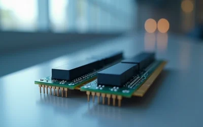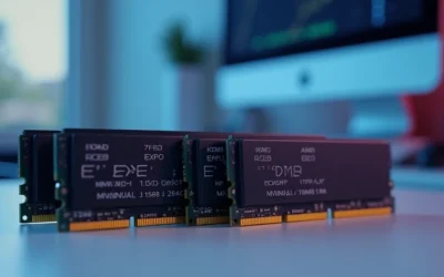

DDR5 ships with conservative JEDEC Memory Standards Specification defaults designed for guaranteed compatibility across every motherboard and silicon combination on the market — not for maximum gaming performance. Tightening sub-timings exploits the headroom manufacturers leave on the table, cutting memory latency by 8–18 ns in real-world tests and translating that directly into higher minimum frame rates in CPU-bound scenarios. This guide covers the full process: identifying your DRAM die, reading the timing chain, adjusting secondary and tertiary parameters safely, validating stability, and reaching a tune that holds across thermal cycles without corrupting data or crashing out of games.
Quick Answer
To tighten DDR5 sub-timings: identify your DRAM die (Hynix A-die, M-die, Samsung B-die, or Micron), enable XMP/EXPO, then reduce tRCD, tRP, tRAS, tRC, tRFC, tWR, and tCWL incrementally in BIOS. Validate with OCCT and y-cruncher. Expect 8–15 ns latency reduction and 3–8% higher 1% lows in CPU-bound titles.

Why Sub-Timings Matter More Than Raw Frequency on DDR5
Most enthusiasts chase DDR5-7200 or DDR5-8000 speeds and stop there, treating sub-timings as secondary. That framing is backward. Frequency determines raw bandwidth; timings determine how quickly the memory controller can issue a command and receive valid data. In gaming — where scene traversal, physics ticks, and draw-call dispatch are serialized latency-sensitive operations — memory latency (measured in nanoseconds, not MT/s) is the dominant variable. A DDR5-6000 CL28 kit tightened to CL26 with aggressive secondaries will routinely outperform a DDR5-7200 CL36 kit at JEDEC defaults in titles like Cyberpunk 2077, Total War: Warhammer III, and Baldur’s Gate 3, which all stress the CPU-memory interface heavily.
The sub-timing chain on DDR5 is longer than DDR4 because the standard introduced on-die ECC, a wider 64-bit channel split into two independent 32-bit sub-channels, and higher base voltages. Those architectural changes mean primary CAS latency (tCL) alone tells you almost nothing. You need to audit the full second-level and third-level timing tree to extract real performance gains. If you are also evaluating platforms, the AMD Ryzen 5 9600X vs Intel Core Ultra 5 245K comparison illustrates how dramatically memory tuning impacts relative CPU performance rankings — the delta between tuned and untuned DDR5 can flip benchmark results between those two processors.
Latency vs. Bandwidth: The Real Trade-off
Tightening timings often costs a small amount of maximum sequential bandwidth because tighter command-to-data delays force the controller to pace bursts more conservatively. Acceptable trade-off for gaming: sacrificing 2–4 GB/s of peak read bandwidth to cut 10 ns off measured AIDA64 latency is always the correct direction for frame-time consistency. Reserve high-bandwidth loose-timing tuning for content creation, video encoding, and memory-intensive HPC workloads where throughput eclipses latency in importance.
Identifying Your DDR5 DRAM Die Before Touching Any Setting
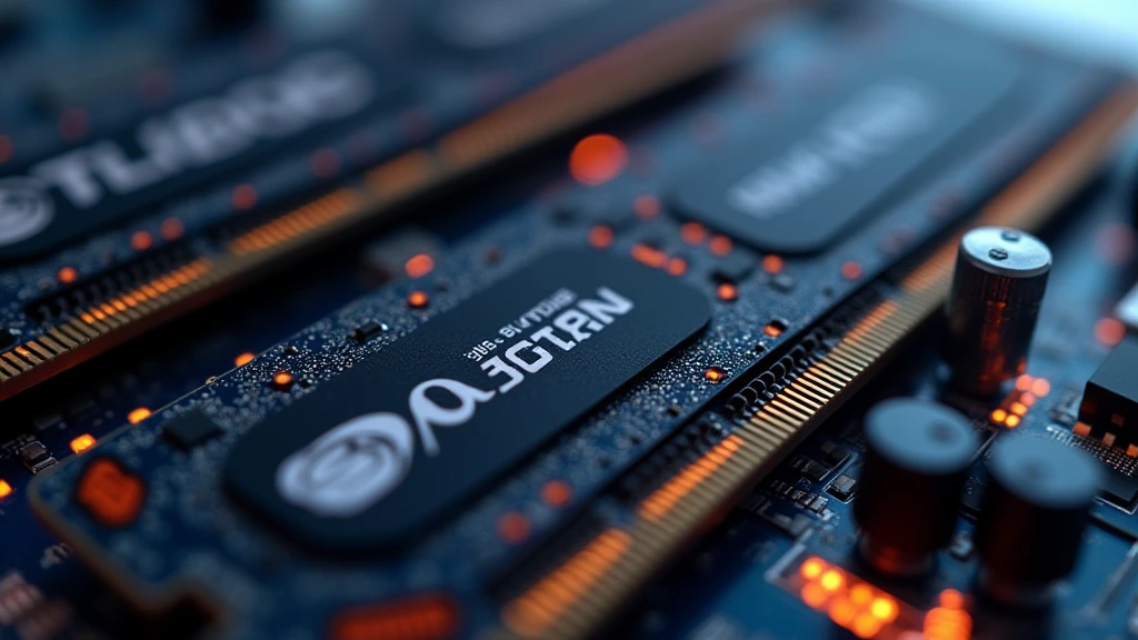
Every major DDR5 DRAM die has a distinct timing behavior profile. Applying Samsung B-die timing presets to Hynix A-die sticks will result in immediate boot failure or, worse, silent data corruption that only surfaces under sustained load. Correct die identification is non-negotiable before you tighten a single sub-timing.
Tools and Methods for Die Identification
- CPU-Z (v2.11+): Reports SPD manufacturer and die revision on the SPD tab. Cross-reference the DRAM manufacturer field with the IC revision string.
- Thaiphoon Burner: Most precise tool for DDR5 SPD decoding. Reads the full 1024-byte SPD EEPROM and reports die part number, revision, and density configuration.
- Visual inspection: Remove the heatspreader on bare-die kits. Hynix A-die (AJR) and M-die (MJR) carry distinct laser-etched part codes; Samsung B-die shows K4 prefix strings on the DRAM IC package.
- Vendor kit lookups: G.Skill, Corsair, and Kingston publish die source lists for specific SKUs on their product support pages.
Die-Specific Timing Characteristics
| DRAM Die | Freq. Sweet Spot | Tight tCL Floor | tRFC Sensitivity | Voltage Headroom | Latency Gain Potential |
|---|---|---|---|---|---|
| Hynix A-die (AJR) | DDR5-6000 – 6800 | CL26 | High — do not go below 295 ns | 1.35 V – 1.45 V | Moderate (8–12 ns) |
| Hynix M-die (MJR) | DDR5-7200 – 8000 | CL28 | Moderate — 310 ns safe floor | 1.40 V – 1.55 V | High (12–18 ns) |
| Samsung B-die | DDR5-6400 – 7200 | CL24 | Low — tolerates 280 ns | 1.30 V – 1.50 V | Very High (14–18 ns) |
| Micron B-die | DDR5-5600 – 6400 | CL28 | High — keep at or above 320 ns | 1.30 V – 1.40 V | Low–Moderate (6–10 ns) |
| Hynix A-die (16Gb) | DDR5-6400 – 7600 | CL26 | High — 340 ns minimum recommended | 1.40 V – 1.50 V | Moderate (10–14 ns) |
The Full DDR5 Sub-Timing Chain: What Each Parameter Controls
Primary timings (tCL-tRCD-tRP-tRAS) appear prominently in BIOS overclocking menus and marketing specs. Secondary and tertiary timings are buried under “Advanced Memory Settings,” “Memory Expert Mode,” or equivalent menu labels depending on whether you are running an Intel Z890-series board or an AMD X670E/X870E platform. Boards like those compared in the ASUS ROG Maximus Z890 Hero vs MSI MEG Z890 ACE comparison expose substantially different levels of timing granularity, with the ROG Maximus exposing full third-level tertiary timing control including tRDWR and tWRRD burst spacing parameters that cheaper boards lock to AUTO.
Primary Timings — Establish the Baseline
- tCL (CAS Latency): Clock cycles from column address strobe to data output. Directly sets perceived read latency. Reduce by 2 from XMP value as first step.
- tRCD (RAS to CAS Delay): Row activation to column access delay. Set equal to or 1 cycle higher than tCL. Too low causes row activation errors under sustained access patterns.
- tRP (Row Precharge Time): Time to precharge a row before activating another. Match to tRCD on most DDR5 dies. Asymmetric values (tRCD u2260 tRP) add instability risk on Hynix A-die.
- tRAS (Row Active Time): Minimum time a row stays active. Safe floor: tCL + tRCD + 4 cycles. Going tighter causes read-to-precharge violations and row hammer false positives.
Secondary Timings — High-Impact Gaming Parameters
- tRC (Row Cycle Time): tRAS + tRP. Reduce only after tRAS and tRP are stable. Aggressive tRC cuts bandwidth latency on burst transfers.
- tRFC (Refresh Cycle Time): Most impactful single secondary timing for DDR5. Controls how long a DRAM row refresh operation takes. Tight tRFC values (280–340 ns depending on die) cut latency 4–7 ns alone. Never tighten without die-specific floor reference — data corruption is the failure mode, not a crash.
- tWR (Write Recovery Time): Cycles after a write before a precharge can issue. Set to tCL + 2 as starting point for most dies, then reduce by 1 each iteration.
- tCWL (CAS Write Latency): Write equivalent of tCL. Match to tCL – 2 on DDR5. Mismatch between tCL and tCWL introduces write timing violations detectable only under sustained random-write workloads.
- tRRD_L / tRRD_S (Row-to-Row Delay, Long/Short): Controls timing between activating different rows in the same/different bank groups. DDR5 sub-channel architecture makes tRRD_S highly impactful. Safe starting reduction: subtract 1 from XMP value.
- tFAW (Four Activate Window): Maximum of four row activations within this window. Cutting tFAW below die minimums causes activation pipeline stalls detectable as latency spikes in AIDA64 random-access measurements.
Tertiary Timings — Fine-Tuning for Enthusiast Builds
Tertiary timings including tRDWR, tWRRD, tWRWR, tRDRD govern burst-to-burst turnaround delays between read and write operations crossing bank group boundaries. On AM5 platforms running DDR5-6000 at the 1:1 MCLK:UCLK ratio — the critical Infinity Fabric sweet spot — tightening tRDWR_sg and tWRRD_sg from AUTO (typically 14–16 cycles) down to 10–12 cycles measurably reduces frame-time variance in games issuing mixed read/write traffic to the memory controller. Enabling gear mode correctly (Gear 1 below DDR5-6400, Gear 2 at or above on most platforms) is prerequisite to stable tertiary timing reduction. Running Gear 2 with Gear 1 tertiary values is a reliable path to memory training failures.
Step-by-Step Tightening Process
This process applies to AMD AM5 and Intel LGA1851 platforms equally. Adjust BIOS menu paths to match your specific board. Refer to desktop CPU benchmarks & reviews to understand how platform-level memory controller differences affect the safe ceiling for these adjustments across processor generations.
- Boot into BIOS, load XMP/EXPO profile. Confirm POST stability with stock XMP before touching any sub-timing. Run OCCT Memory (1 hour, SSE2) to validate the XMP baseline — do not skip this step.
- Record all current timing values. Screenshot or photograph every value under Advanced Memory Settings. AUTO-computed values will disappear once you begin manual overrides and cannot be recovered without a CMOS reset.
- Reduce tCL by 2, leave all others at AUTO. Boot, run y-cruncher (VT3 test, 15 minutes). Fail = increment tCL back by 1, verify VDIMM is at XMP spec.
- Match tRCD and tRP to new tCL. Boot test as above. If unstable at matched values, set tRCD = tCL + 1.
- Set tRAS to tCL + tRCD + 4. Recalculate after each primary timing change.
- Reduce tRFC by 20 ns increments using die-specific floor from the table above. Each reduction: run TestMem5 (anta777 extreme preset, 3 passes). Any error: increment tRFC by 10 ns, re-test.
- Reduce tWR by 1 cycle. Test with OCCT Memory Large (30 minutes). Stable: proceed. Fail: revert.
- Tighten tRRD_L and tRRD_S by 1 cycle each. Run AIDA64 cache/memory benchmark 5 consecutive passes — verify latency drops without bandwidth regression exceeding 3%.
- Final stability gauntlet: 4-hour OCCT Memory + 2-hour y-cruncher + 1 hour Prime95 (In-Place FFTs, all cores). Any error at any stage: revert the last changed parameter by the smallest increment and re-run full gauntlet.
Voltage Settings During Sub-Timing Tightening
Tighter timings require adequate VDIMM and VDDQ to meet setup/hold timing margins. For Hynix A-die tighten-to-CL26 targets, 1.40 V VDIMM with VDDQ matched is the reliable entry point. Samsung B-die CL24 targets often train stable at 1.45–1.50 V. Do not exceed 1.55 V VDIMM on DDR5 without active airflow across the DRAM ICs — JEDEC specifies 85°C as the maximum operating junction temperature for DDR5 ICs, and voltage-induced thermal runaway above 1.55 V at ambient temperatures above 30°C is a documented failure mode. Monitor DRAM temperatures with HWiNFO64 throughout all test sessions. The GPU subsystem thermal environment also affects ambient case temperature during gaming; consult the Radeon RX 9060 XT 8GB vs 16GB comparison for real-world thermal output data from a current-generation mid-range GPU that will co-exist with your memory inside the same chassis. For additional GPU thermal context across the full stack, see graphics card tests & GPU guides.
Measuring Real-World Gaming Latency Gains
Benchmarking memory sub-timing changes demands consistent, repeatable measurement methodology. AIDA64 memory latency (the single most important synthetic metric), CapFrameX frame-time capture during in-game benchmark runs, and FRAMEDROP analysis across a fixed 60-second sequence are the three mandatory data capture points.
Expected Gains by Profile
- XMP only (no sub-timing work): Baseline reference. AIDA64 latency typically 75–90 ns at DDR5-6000 CL36 JEDEC default.
- Primary timings tightened (CL28 u2192 CL26): 5–8 ns latency reduction, 1–3% 1% low improvement in CPU-bound titles.
- Primary + secondary (tRFC, tWR, tRRD tightened): 10–15 ns total latency reduction, 3–6% 1% low improvement.
- Full primary + secondary + tertiary tune: 14–18 ns latency reduction versus XMP default, 5–9% 1% low improvement. Results most pronounced in open-world CPU-bound titles at 1080p–1440p with a fast GPU.
Final Diagnostic Verdict & Maintenance Checklist
A complete tighten-ddr5-sub-timings process executed correctly produces a stable, lower-latency system that holds its tune across thermal cycles, BIOS updates, and long gaming sessions. The failure modes — training failures, blue screens under sustained load, sporadic application crashes — all trace back to one of three root causes: insufficient VDIMM for the timing targets chosen, tRFC set below the die-specific safe floor, or tCWL/tCL mismatch exceeding 2 cycles. This tighten ddr5 sub timings guide resolves all three by requiring verification at each incremental step rather than applying community timing sheets blindly — a methodology that accounts for silicon lottery variation within the same die revision. As the pc hardware 2026 platform landscape matures with Z890 and X870E boards gaining more granular timing control through AGESA and ME firmware updates, the ceiling for what is achievable with consumer DDR5 kits will continue to rise.
- Confirm die identity via Thaiphoon Burner before any BIOS change.
- Save BIOS profile after each stable milestone — not only at final tune.
- Revalidate full stability gauntlet after every BIOS firmware update (AGESA updates routinely change memory training algorithms, invalidating previously stable timing tables).
- Monitor DRAM junction temperature with HWiNFO64 during first week of gameplay — target below 75°C under sustained gaming load.
- Run OCCT Memory (30 minutes) monthly if running VDIMM above 1.45 V — higher voltages accelerate DRAM cell wear and sub-timing stability can drift over months.
- Document every changed parameter with exact values in a plain-text file stored outside the OS drive — CMOS resets are inevitable over a system’s lifespan.
- Do not tighten sub-timings after a CPU, motherboard, or DRAM swap without restarting the entire identification and validation process from step 1 — silicon-to-silicon memory controller impedance variation makes cross-component timing portability unreliable.